LCD SPI initialization coding part-2
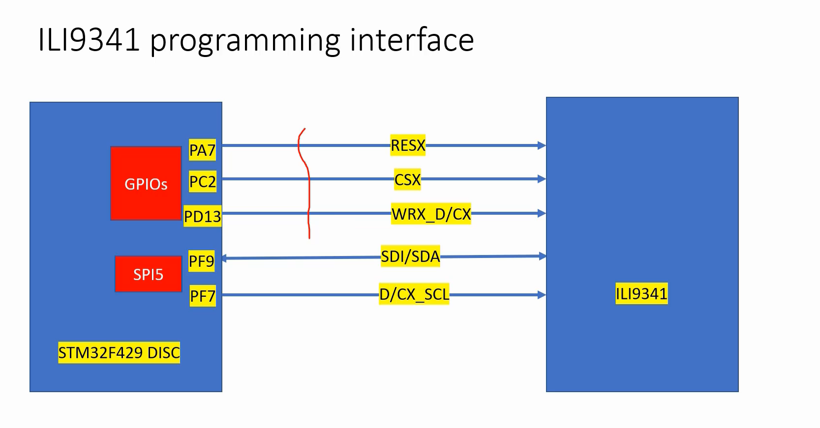
We defined all the required LCD signals for our exercise.
#include "stm32f429xx.c"

/*Define all the LCD signals */

#ifdef STM32F429I_DISC1

    #define SPI                                       SPI5

    #define LCD_SCL_PIN                               GPIO_PIN_7

    #define LCD_SCL_PORT                              GPIOF

    #define LCD_SDA_PIN                               GPIO_PIN_9

    #define LCD_SDA_PORT                              GPIOF

    #define LCD_RESX_PIN                              GPIO_PIN_7

    #define LCD_RESX_PORT                             GPIOA

    #define LCD_CSX_PIN                               GPIO_PIN_2

    #define LCD_CSX_PORT                              GPIOC

    #define LCD_DCX_PIN                               GPIO_PIN_13

    #define LCD_DCX_PORT                              GPIOD

#elif defined(STM32F407)

    #define SPI                                        SPI2

    #define LCD_SCL_PIN                                GPIO_PIN_13

    #define LCD_SCL_PORT                               GPIOB

    #define LCD_SDI_PIN                                GPIO_PIN_15

    #define LCD_SDI_PORT                               GPIOB

    #define LCD_SDO_PIN                                GPIO_PIN_2

    #define LCD_SDO_PORT                               GPIOC

    #define LCD_RESX_PIN                               GPIO_PIN_10

    #define LCD_RESX_PORT                              GPIOD

    #define LCD_CSX_PIN                                GPIO_PIN_11

    #define LCD_CSX_PORT                               GPIOD

    #define LCD_DCX_PIN                                GPIO_PIN_9

    #define LCD_DCX_PORT                               GPIOD


#else

          #error"Supported device is not selected"

#endif
Here, you can see that we have used different names for the DCX signal. However, there are still some differences in the SDA. In the STM32F429I_DISC1 section, we have used the name SDA, whereas, in the STM32F407, we have two names: SDI and SDO.
In this article, we will implement the BSP_LCD_Init function. This function first requires us to initialize the pins. Therefore, we will need to initialize all the pins. After that, we will need to initialize the SPI. To accomplish this, we will define the SPI using the #define SPI macro, as shown above.
#define SPI SPI5
#define SPI SPI2
Next, we will implement helper functions such as LCD_Pin_init(), LCD_SPI_init(), LCD_Reset(), and LCD_Config(). These functions are static and will assist in initializing the pins, and SPI, resetting the LCD and configuring it by sending commands.
Specifically, we will use LCD_Pin_init() for pin initialization, and SPI initialization. After initialization, we will reset the LCD and configure it by sending the necessary commands.
First, we need to initialize the RESX, CSX, and DCX pins for the output mode. Allow me to briefly explain the steps required to configure these pins for GPIO output mode.
Let’s consult the reference manual to determine the necessary actions. Firstly, by examining the memory map(Figure 2), we can identify that the GPIOs are usually connected to the AHB1 domain. Therefore, before you configure any registers of these peripherals, you have to enable the clock for these peripherals.
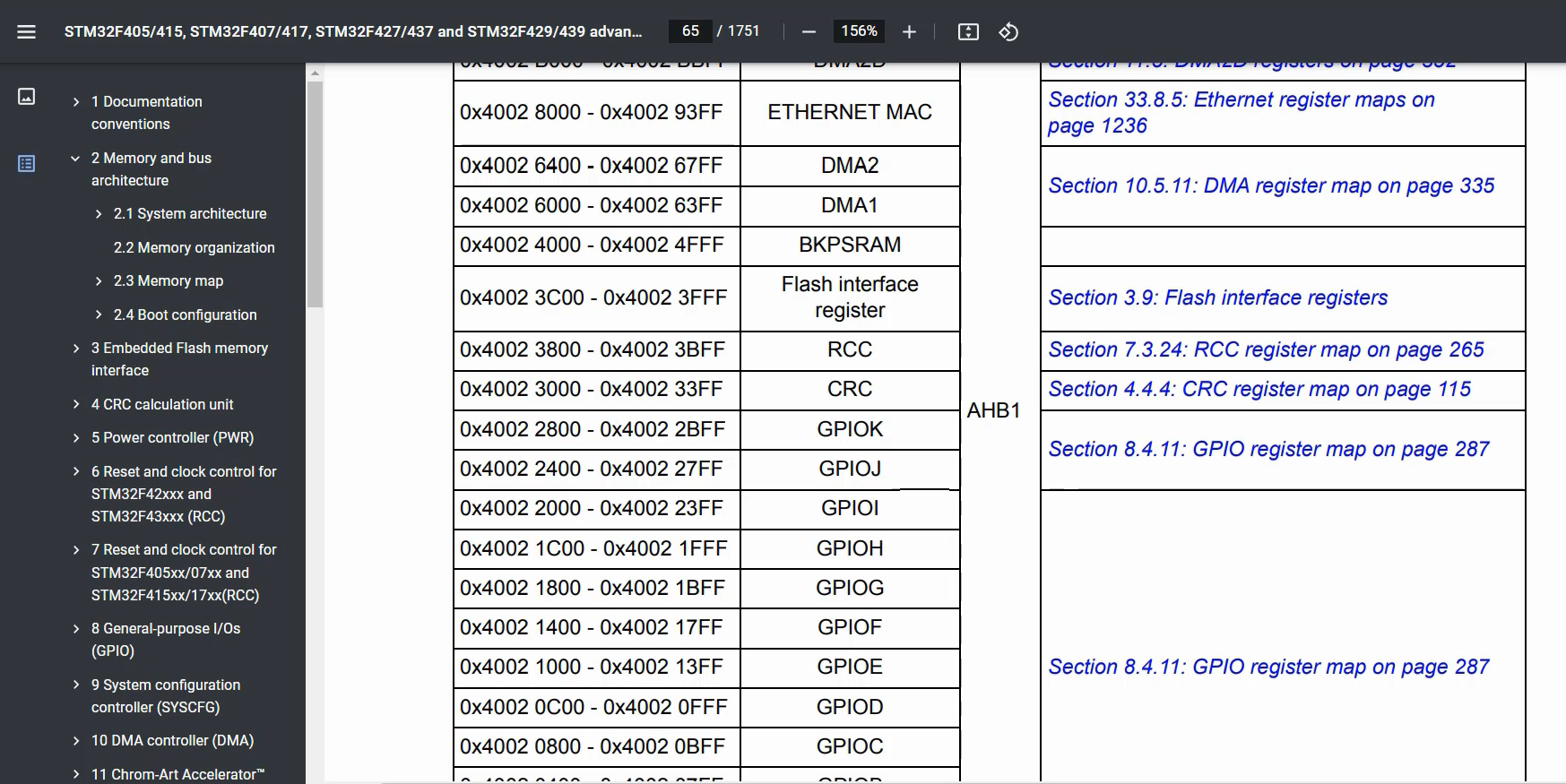
As I am working with GPIOs, I will navigate to the AHB1 peripheral clock register (AHB1ENR). And here you have to turn on the clock for the peripheral which you want to use.
To do so, one must access the clock enable register found within the RCC AHB1 peripheral clock register (RCC_AHB1ENR).
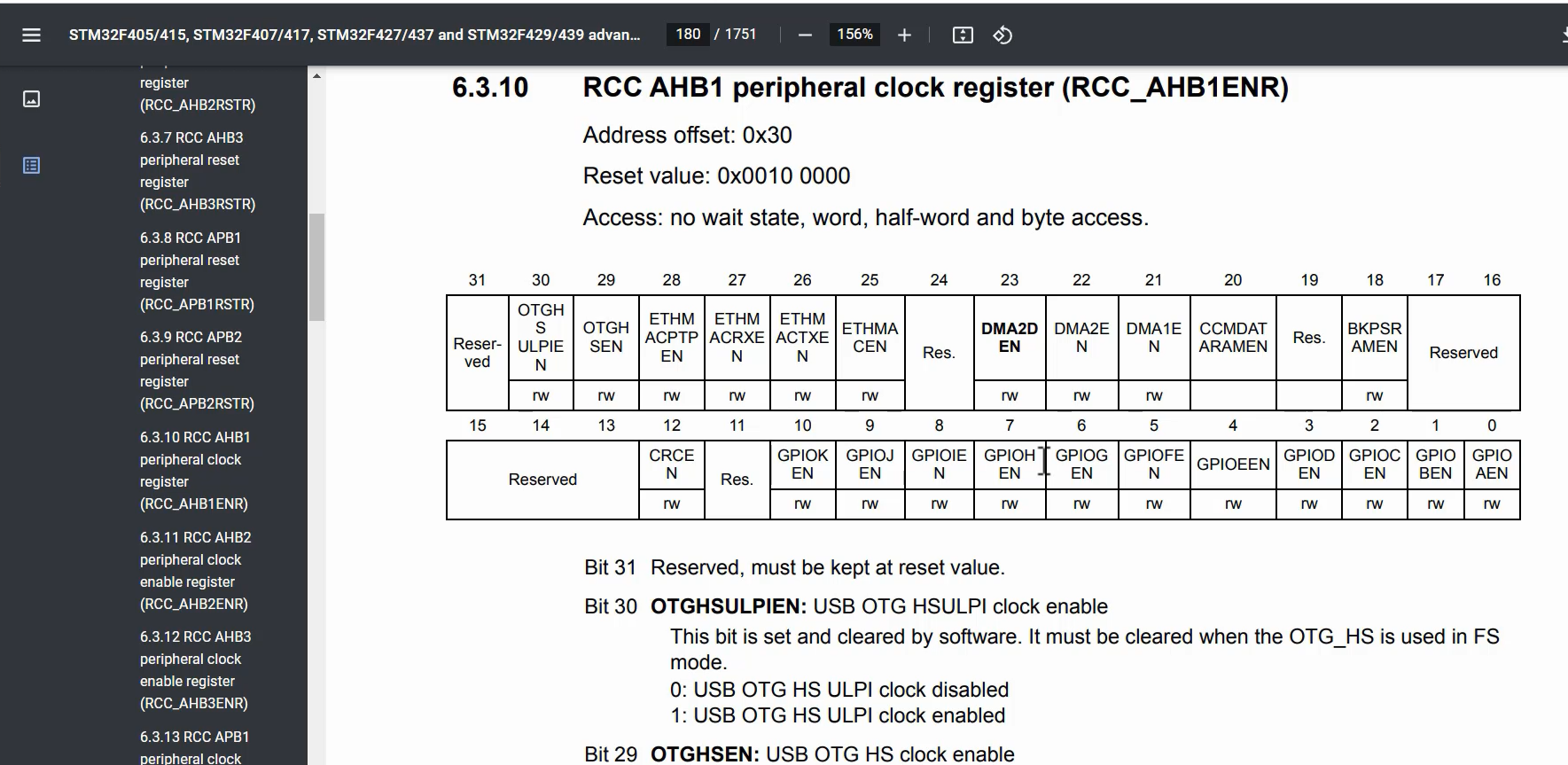
First, let’s begin with the RESX pin, which can be found on PA7, a GPIO port. Since we will be utilizing GPIO ports A, C, D, and F, it is essential to activate the clock for all these peripherals by selecting the appropriate bits from the RCC_AHB1ENR register. That’s the first thing you have to do.
Next, you must configure the RESX, CSX, and DCX pins to output mode. To do this, navigate to the GPIO section, locate the mode register, and choose the general-purpose output mode.
To summarize, start by enabling the clock for the necessary peripherals, and then configure the pins to output mode.
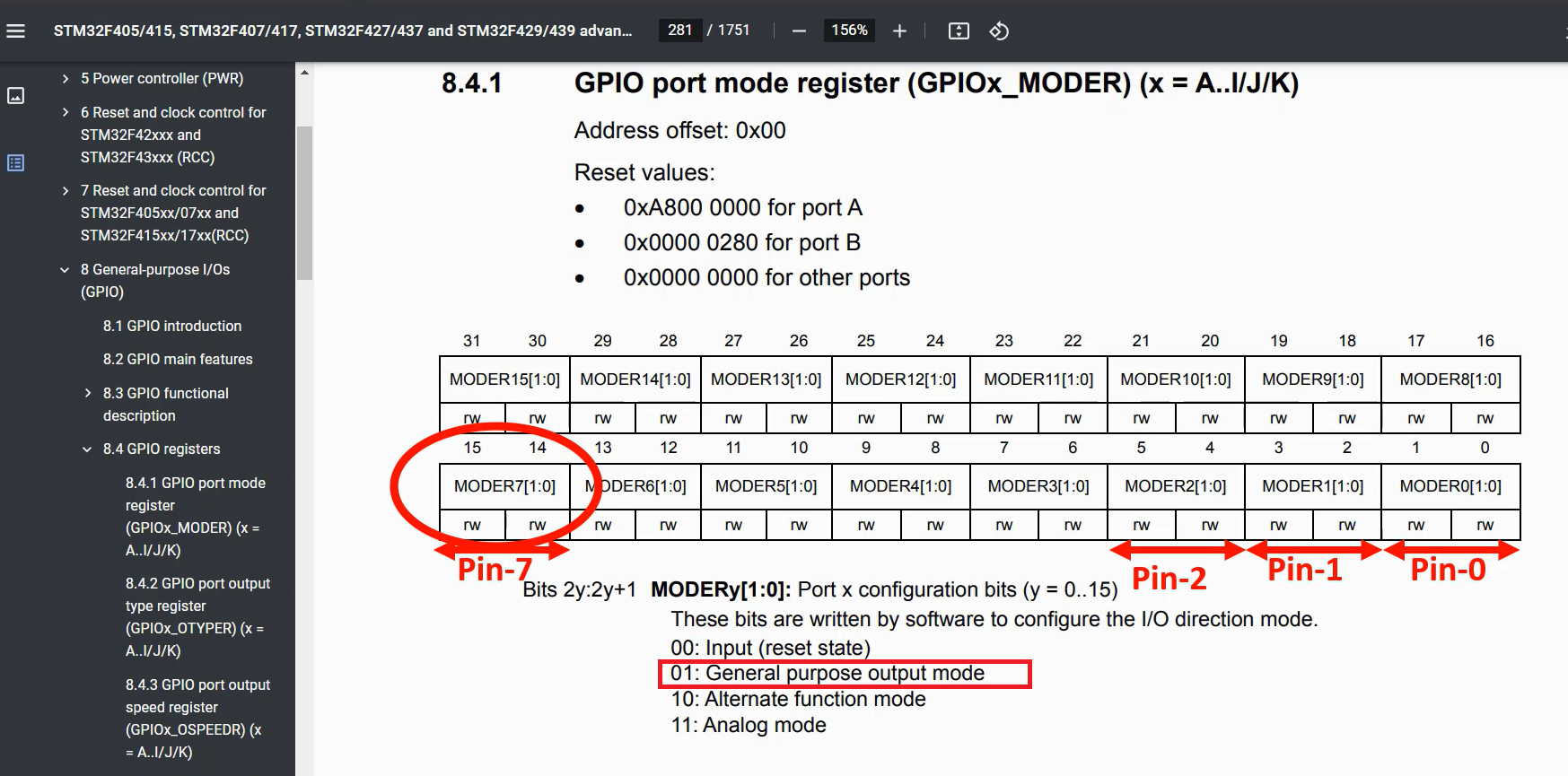
So, just feed the appropriate value into these bit fields. You can use the REG_SET_VAL macro, which you used before.
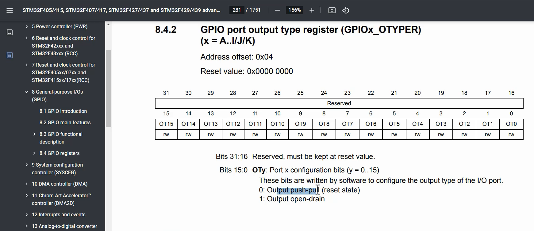
After that, we need to consider the output type. As previously mentioned, we want to use push-pull, no open drain things here. Therefore, we won’t be utilizing any external or internal pull-ups or pull-downs. Our goal is simply to control the signal’s ON and OFF states.
The GPIO port output speed register(GPIOx_OSPEEDR). So, it doesn’t matter actually, set it for high speed.
Let’s code for one pin. The following code is related to configuring one GPIO pin.
First start with REX, which is PA7.This indicates that the pin being configured is PA7. PA7 is a specific pin on the microcontroller that is being programmed.
Before this will just turn on the clock. So, before configuring the pin, the clock needs to be enabled for the GPIO port to which the pin belongs. This is necessary for the pin to function correctly.
Let’s add the header file #include “reg_util.h”. This line includes the header file “reg_util.h”, which provides definitions for Register Access Macros that will be used later in the code.
Create one variable → RCC_TypeDef *pRCC = RCC;
Here creates a pointer variable named “pRCC” that points to the RCC (Reset and Clock Control) register in the microcontroller. This register controls the clock system for various peripherals, including GPIO ports.
REG_SET_BIT(pRCC->AHB1ENR, RCC_AHB1ENR_GPIOAEN_Pos);
This line uses the Register Access Macro REG_SET_BIT to set a particular bit in the AHB1ENR (Advanced High-performance Bus 1 Enable Register) of the RCC register. This bit corresponds to the GPIOA port, which is the port to which the PA7 pin belongs. Setting this bit enables the clock for the GPIOA port.
The similar steps need to be followed to enable the clock for the GPIOC and GPIOD ports. The exact code for this is not shown, but it likely involves using the same Register Access Macro to set the appropriate bit in the AHB1ENR register for those ports.
void LCD_Pin_Init(void)
{
RCC_TypeDef *pRCC = RCC;
GPIO_TypeDef *pGPIOA = GPIOA;


/* Enable the clock for GPIOA,C,D peripherals */
REG_SET_BIT(pRCC->AHB1ENR,RCC_AHB1ENR_GPIOAEN_Pos);
REG_SET_BIT(pRCC->AHB1ENR,RCC_AHB1ENR_GPIOCEN_Pos);
REG_SET_BIT(pRCC->AHB1ENR,RCC_AHB1ENR_GPIODEN_Pos);


//REX
REG_SET_VAL(pGPIOA->MODER,0x1U,0x3,GPIO_MODER_MODE7_Pos); /*mode*/
REG_CLR_BIT(pGPIOA->OTYPER,GPIO_OTYPER_OT7_Pos); /*Output type*/
REG_SET_VAL(pGPIOA->OSPEEDR,2U,0x3U,GPIO_OSPEEDR_OSPEED7_Pos); /*speed*/
After identifying the target register, REG_SET_VAL can be used. Before that, which specific register are you trying to modify?
Let’s focus on programming the registers of the GPIOA peripheral. To do so, we need to create a variable that can access the base address of the peripheral. This can be achieved by defining a pointer variable of type GPIO_TypeDef, which we can name as pGPIOA, and assigning it the value of the GPIOA base address.
GPIO_TypeDef *pGPIOA = GPIOA;
Going forward, we need to use this pGPIOA pointer to access the specific registers of GPIOA that we want to modify.
The first register we want to set is the mode register MODER(Figure 4). The value we want to set in this register is 01, which corresponds to the binary value 0x1U. To set this value, we need to use a mask of 0x3, which will only modify the relevant bits in the register.
Since every pin in the GPIOA peripheral takes up 2 bits in the MODER register, we need to identify the correct position of the bits corresponding to the pin we want to modify. For example, for pin 7, we need to use the position GPIO_MODER_MODE7_Pos, which is equivalent to 14.
To configure the mode for GPIO port A, PIN number 7, refer to Figure 5 and locate pin number 7.
Use the available macro, REG_SET_VAL(pGPIOA->MODER, 0x1U, 0x3, GPIO_MODER_MODE7_Pos), to set the mode.
Next, choose the output type Push-pull by referring to Figure 6. Since every pin takes a single bit and it needs to be 0, simply use the clear bit by using the register pGPIOA->OTYPER and GPIO_OTYPER_OT7_Pos. Use REG_CLR_BIT to clear the bit:
REG_CLR_BIT(pGPIOA->OTYPER, GPIO_OTYPER_OT7_Pos);
To set the speed, use REG_SET_VAL and the register pGPIO->OSPEEDR with a value of 2. Then, (0x3). The position is available with GPIO_OSPEEDR_OSPEED7_Pos.
Use REG_SET_VAL(pGPIOA->OSPEEDR, 2U, 0x3U, GPIO_OSPEEDR_OSPEED7_Pos) to configure the REX pin to push-pull output.
These steps will configure the REX pin, and you can continue with the remaining pins.
FastBit Embedded Brain Academy Courses
Click here: https://fastbitlab.com/course1

