GPIO behind the scene
In this article, let’s understand how the GPIO pin is implemented inside the microcontroller.

Figure 1 is GPIO looks behind the scene. There is one input buffer, one output buffer, and an enable line. When an enable line is zero, the output buffer gets activated, and the input buffer gets deactivated.
Let’s discuss what actually buffer is.
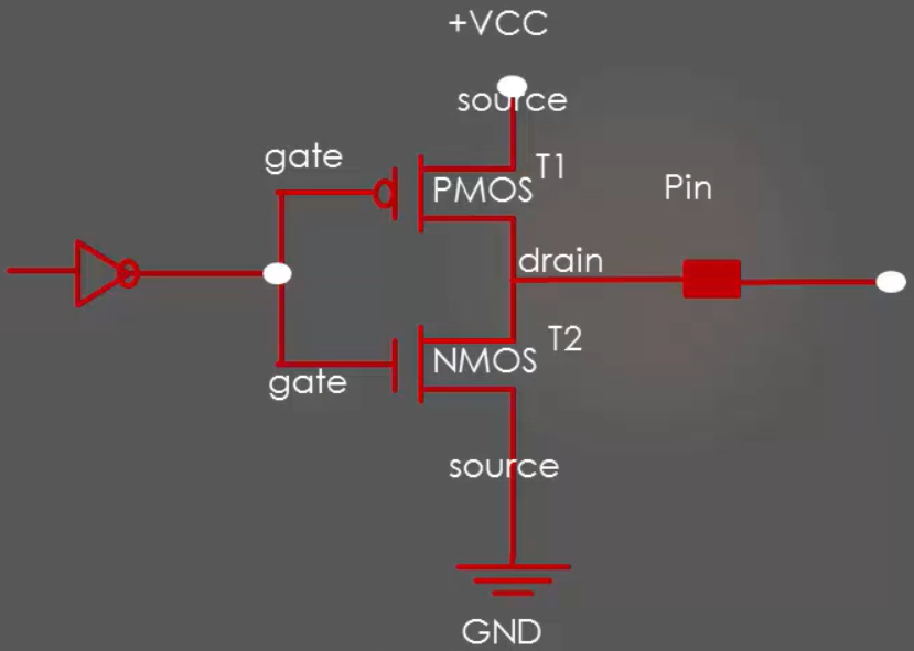
Buffer is nothing but 2 CMOS transistors connected as shown in the Figure 2.

From Figure2. The top one is called the PMOS transistor, and the bottom one is called the NMOS transistor. When you want to write one to this output pin, which feeds 0 to the NOT gate, T1 will get activated, and T2 gets deactivated, and you get one on this microcontroller pin.
If you want to write zero to this pin, which feeds 1 to the NOT gate. T1 gets deactivated, and T2 gets activated, and pin pulled to the ground which gives zero onto the pin. That’s how the output buffer of a GPIO works.
On the other hand, if you make an enable line is equal to one, then you are making a pin to work in input mode by activating input buffer and deactivating output buffer.
Let’s see how the input buffer works.
When the pin is in higher voltage T1 will be ON, and T2 will be OFF. So, a pin is read to high. And when the pin is in low, T1 turns OFF, and T2 conducts and a pin is read to low.
GPIO control registers usually configure an enable line.
In the next article, let’s learn GPIO input mode high impedence state .
FastBit Embedded Brain Academy Courses,
Click here: https://fastbitlab.com/course1


