Exercise: Testing
The I2C trace in Figure 1 is not good because it has some problems. There is a glitch (Figure 2) after every packet transaction.
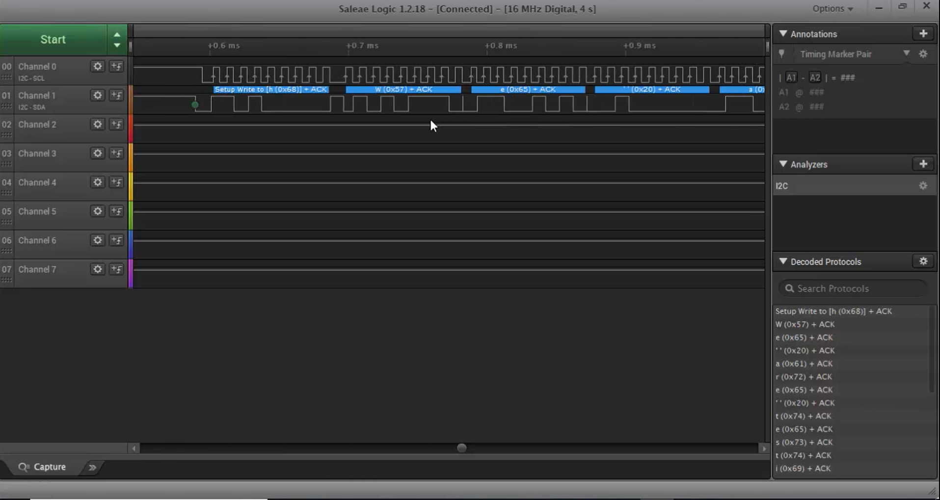
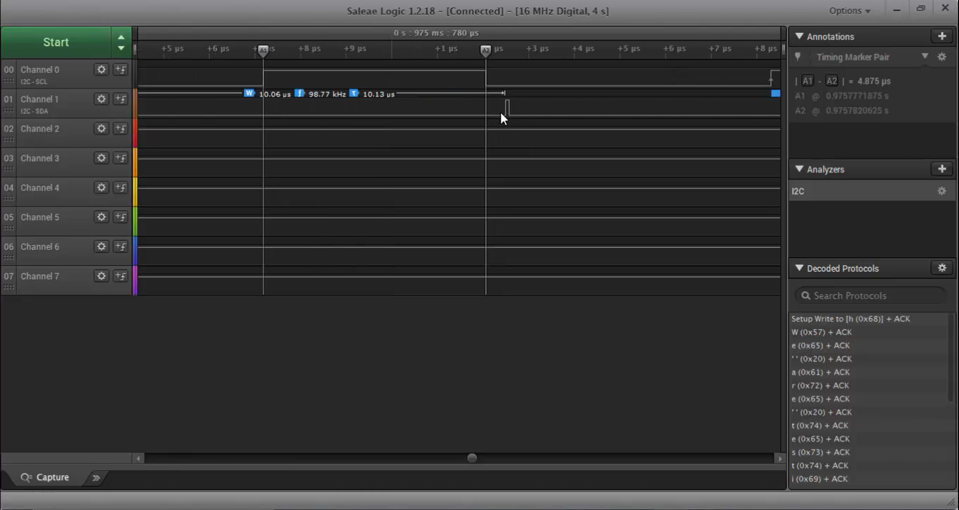
The byte transmission ends at the 8th clock cycle, and 8-bits are transferred. After the 8th clock cycle, there is an ACK. But look at Figure 2. After the ACK, there is a small glitch, which is not good. The glitch is not affecting our expected behavior because the data is being received properly from the slave. Even though the data reception is fine, the glitch should not occur.
Now investigate the reason that causes the glitch to occur. This glitch is happening after every byte transfer, which means the SDA line is pulled to high, and then it is released, and the duration is approximately 125 nanoseconds.
Steps to investigate the reason for glitch:
- Refer to the reference manual to investigate whether there is any special meaning for PB9 or used for any special purpose.
- Go to the reference manual.
- Search the word PB9 in the reference manual. None of the pages of the reference manual talk about the PB9.
- Go to the datasheet and see what the datasheet says about PB9. The datasheet mentioned that the PB9 could be used for SPI2, I2C, timer, alternate functionalities, etc. That means the microcontroller treats PB9 as normal GPIO, and there is no special meaning for that.
- Now investigate the board’s user manual to see whether PB9 is used for any special purpose on board.
- Go to the discovery kit’s board document (the board that I have used in the exercise).
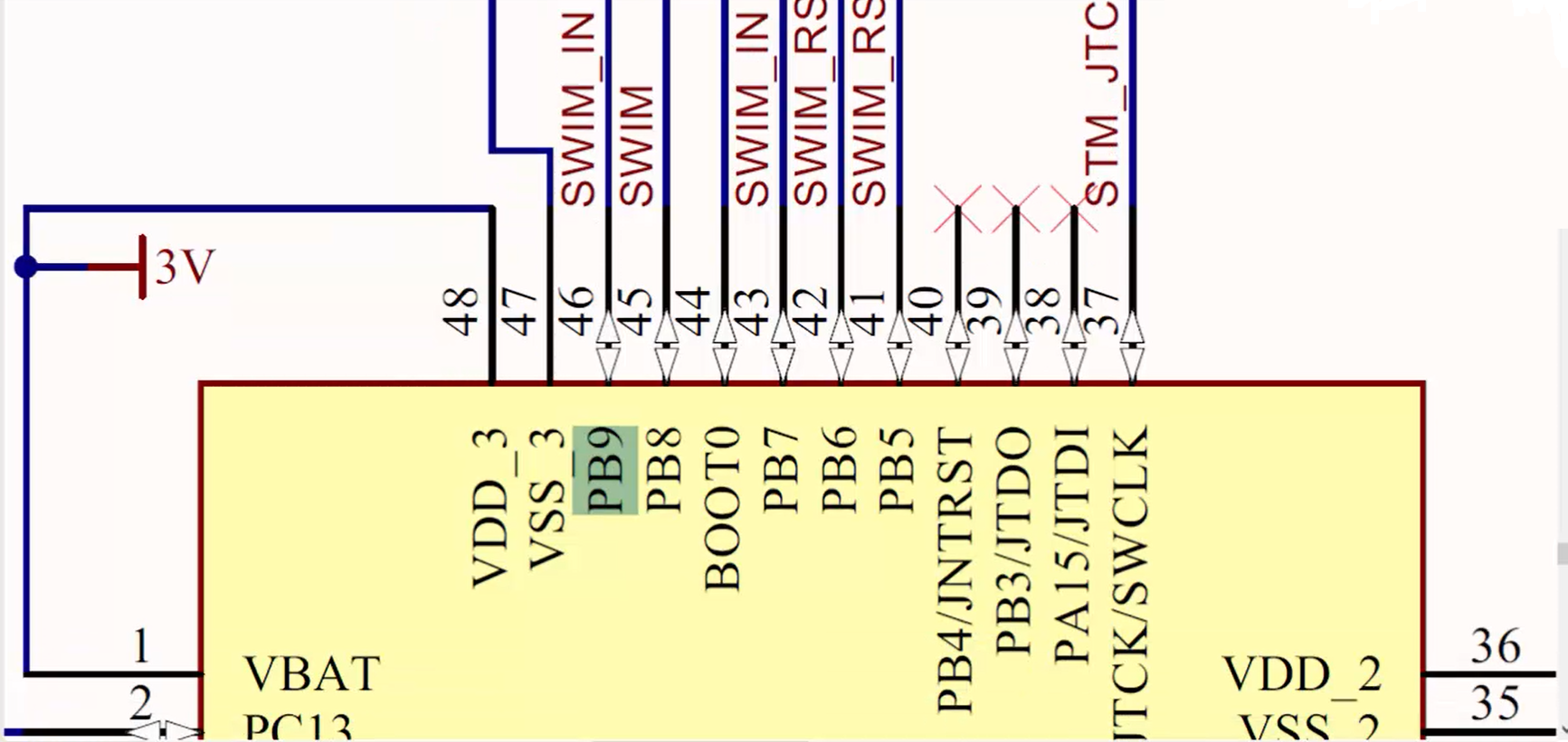
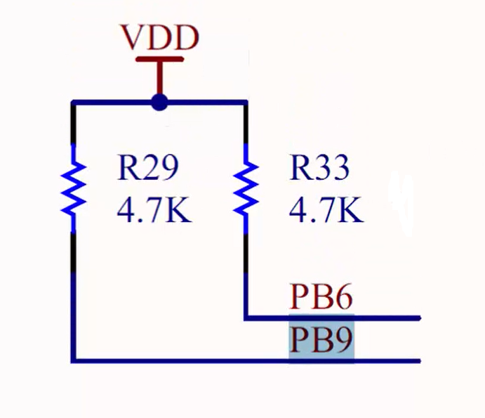
- Search for the word PB9. In Figure 3, you can observe that the PB9 is being used for a SWIM. SWIM stands for Single Wire Interface Module, which is used to program the board, and it is connected to some other circuitry, as shown in Figure 4.
Way to resolve the problem (glitch):
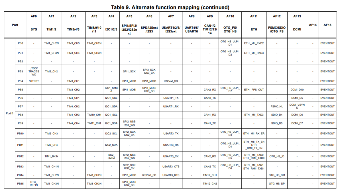
- The SWIM circuitry may be causing that glitch over PB9. So, let’s use another pin instead of PB9. Look at Figure 5. PB7 can also be used as the I2C1_SDA.
- Go to the program and replace the PB9 with PB7, as shown in Figure 6.
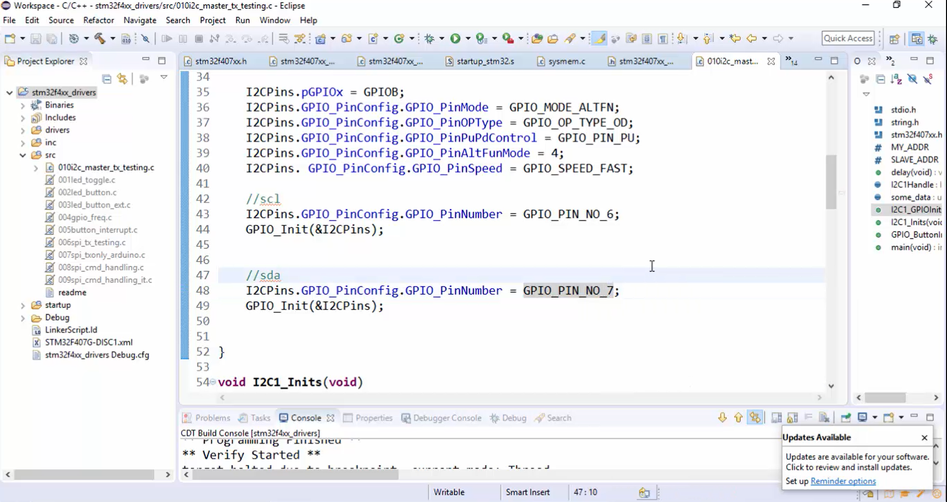
Do this change only if you observe those glitches in the I2C trace.
- Build the project and program the chip.
- Capture the output (Figure 7).
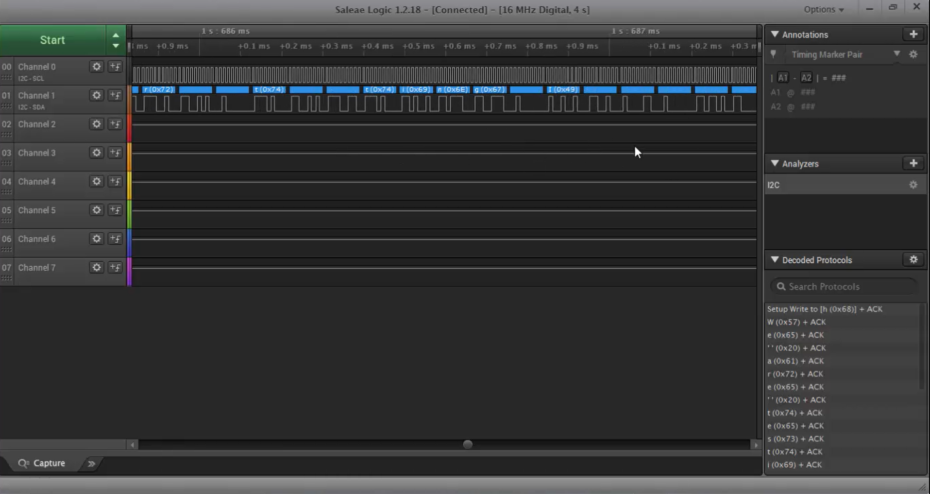
Observe Figure 7. There is no glitch in the trace. The output is immaculate and glitch-free. That means the onboard circuitry is the reason for causing some problems to the PB9.
In the following article, let’s see I2C transfer sequence diagram for master receiving data.
FastBit Embedded Brain Academy Courses,
Click here: https://fastbitlab.com/course1

