Exercise: Coding Part 2
- Compile the code in Figure 1.
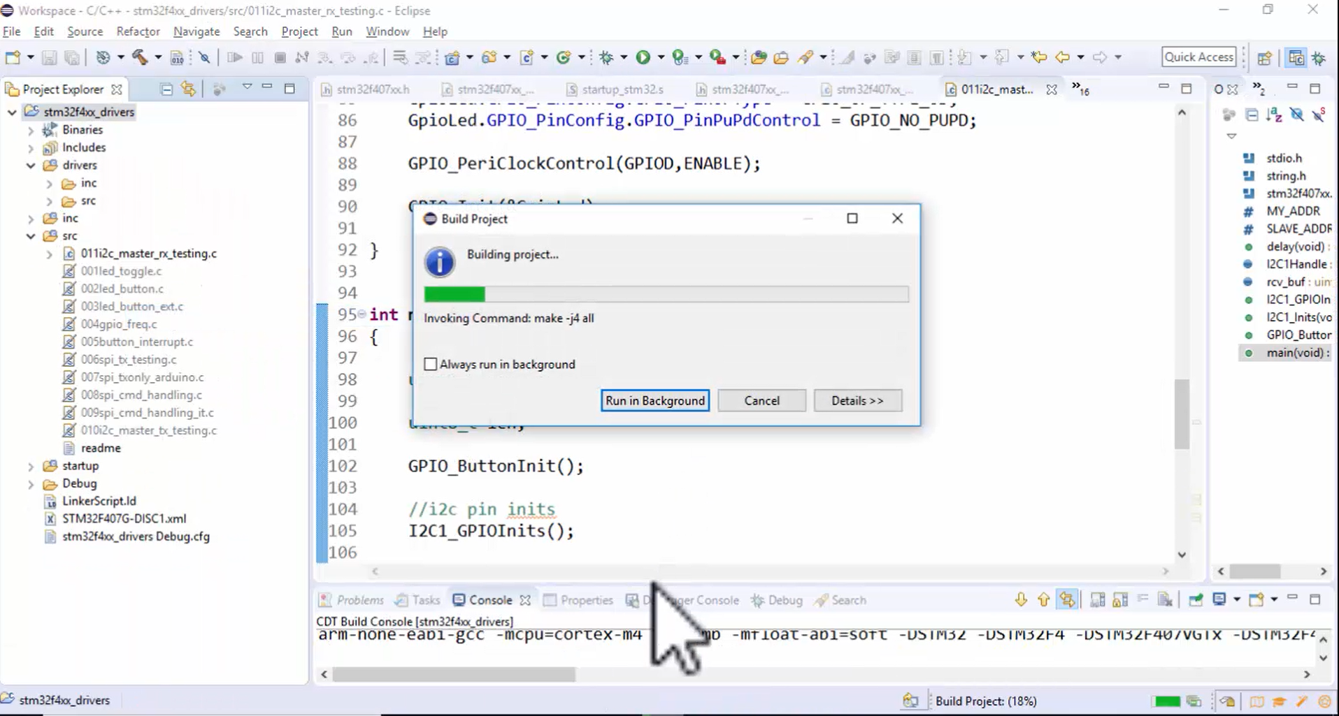
2. Download the code into the board, as shown in Figure 2.
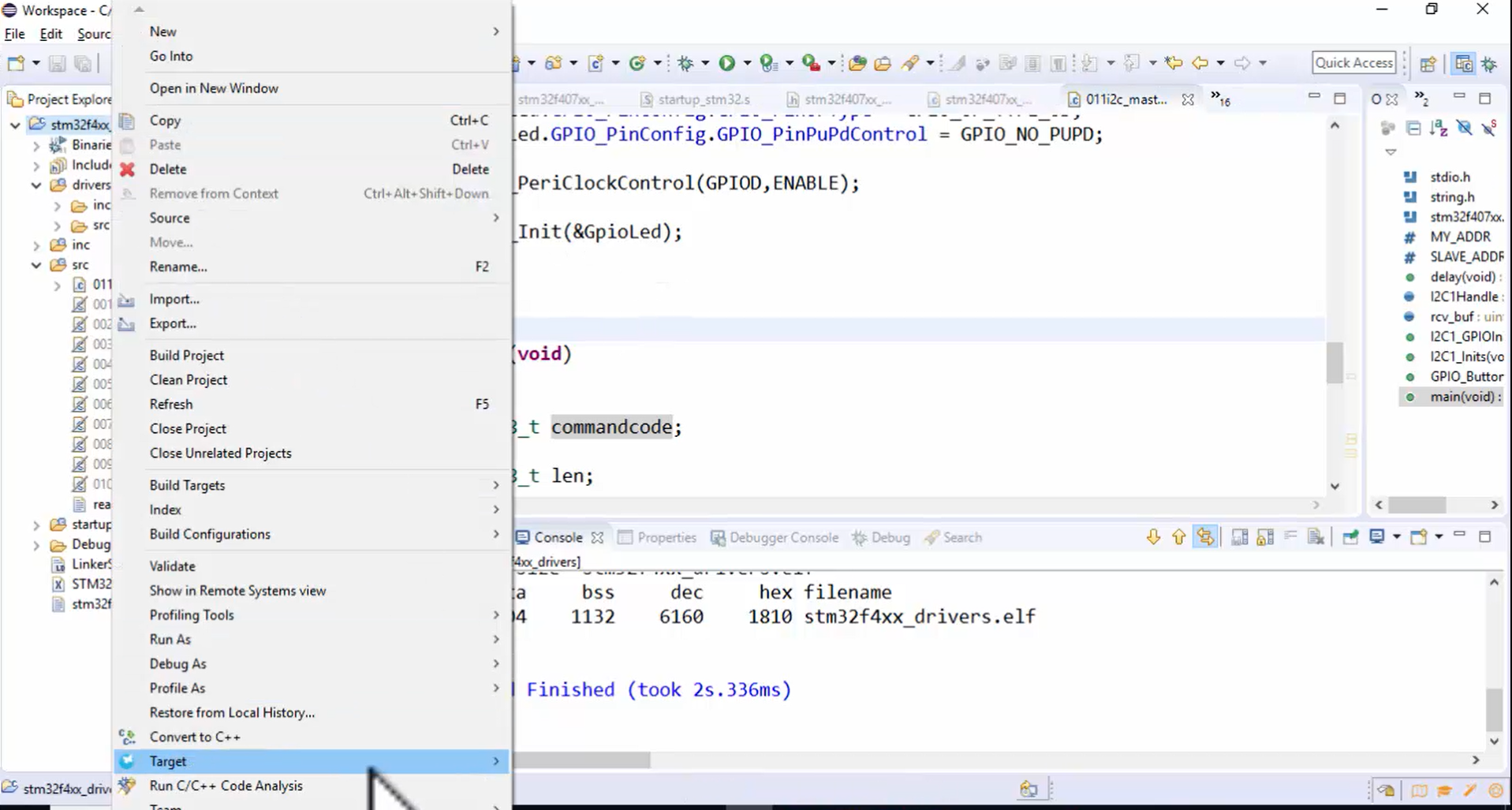
3.Reset both the Arduino and STM board.
4. Open the logic analyzer (Figure 3).
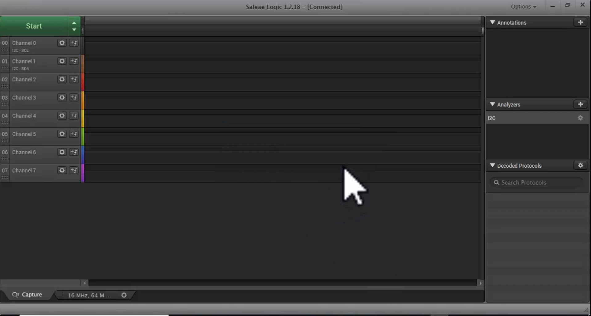
5. Capture the result by pressing the start button.
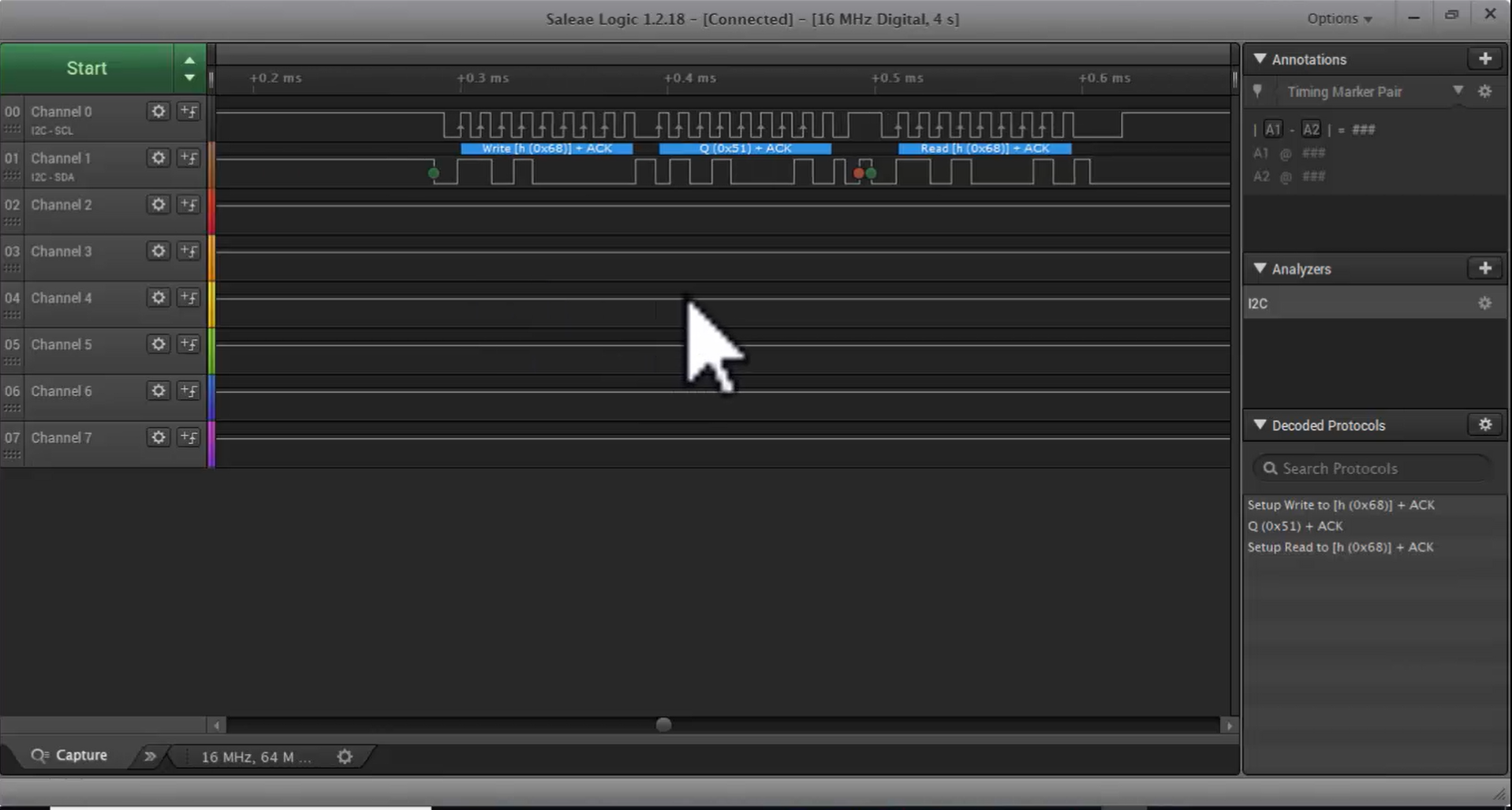
Look at Figure 4. It looks like the application is not working properly.
- There is a start condition.
- After the start condition, there is an I2C write transaction.
- Performing address phase: Master writes a slave address 0x68, as shown in Figure 5.
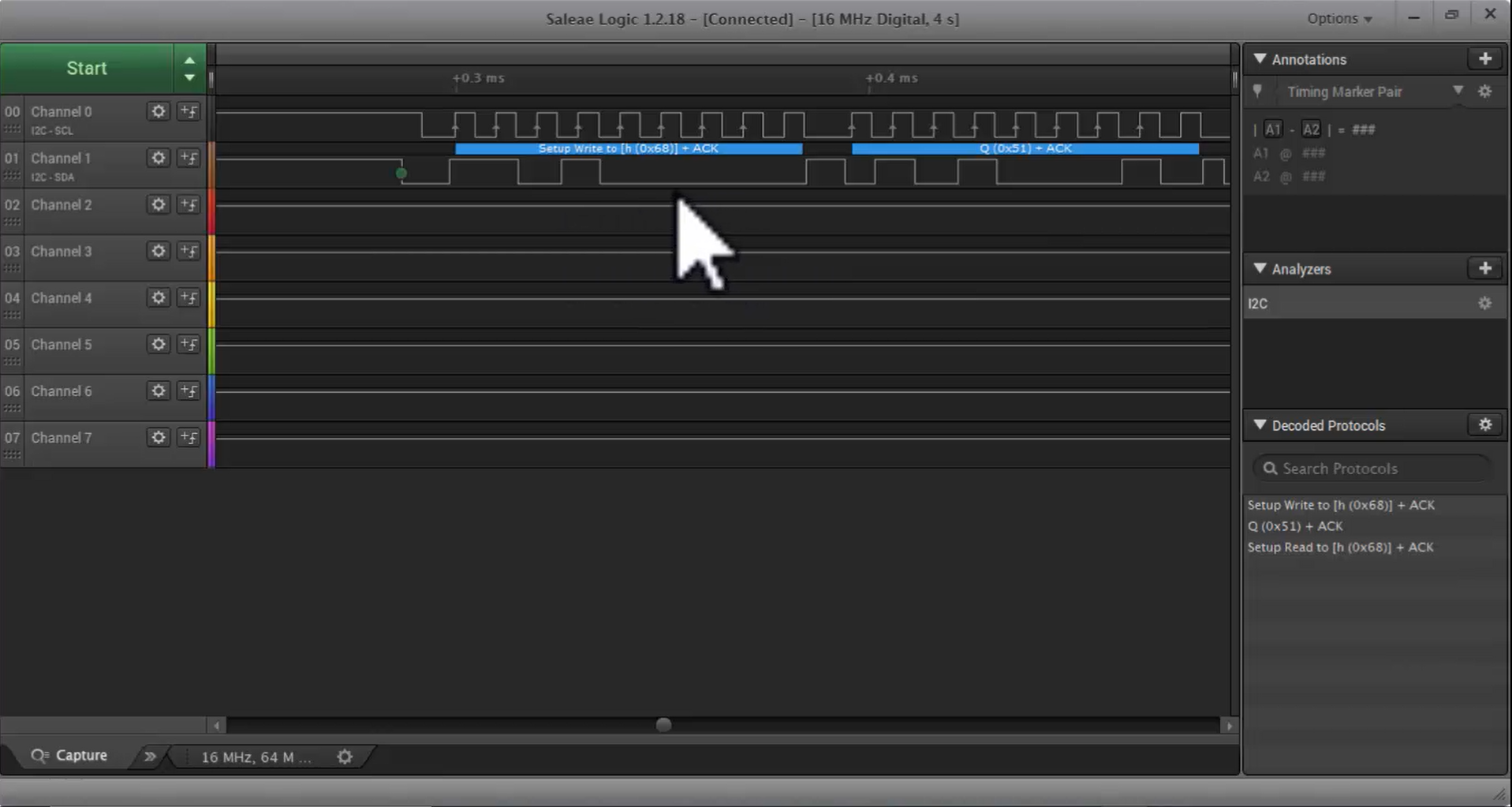
- Then the master sends the command code 0x51.
- The master terminates the I2C transaction by generating the stop condition.
There is no problem with the first transaction.
- To read the data master triggers the read transaction.
- Figure 6 shows the generation of the read transaction. There is no reply from the slave for this transaction, and it looks like the SCL line is pulled to high.
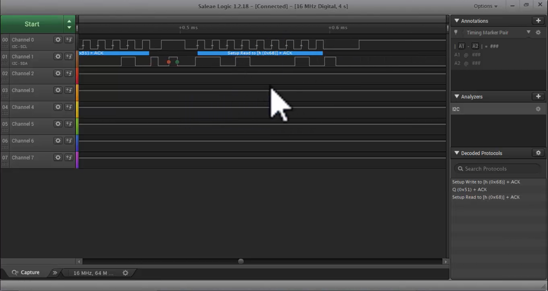
The stop is generated abruptly, as shown in Figure 7, because there is some problem with the driver. This problem may be because of our code.
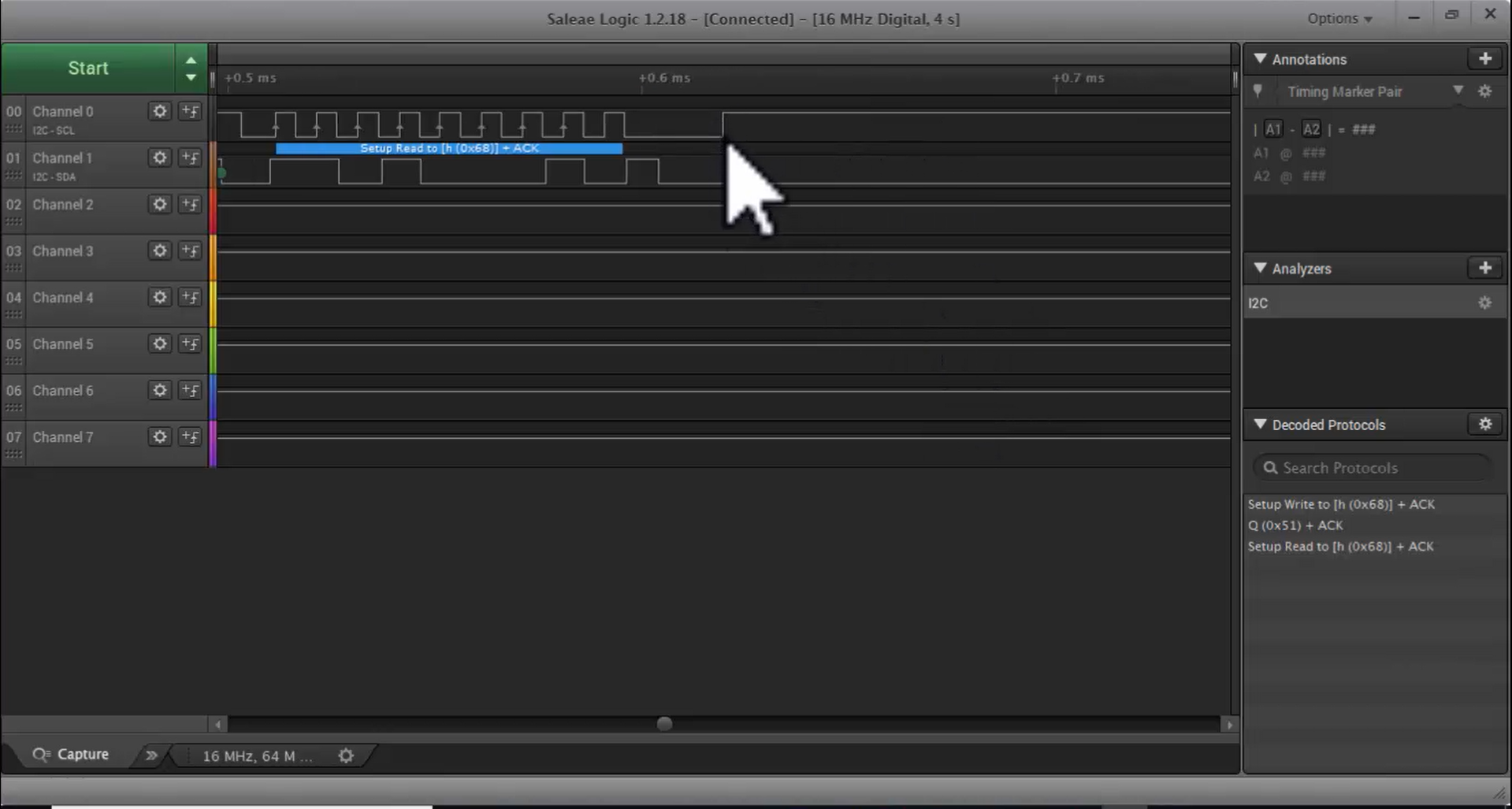
Now let’s make some changes to the code:
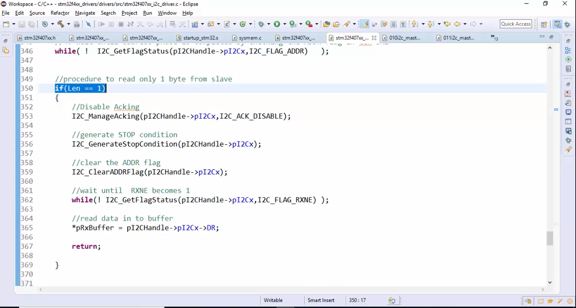
- Observe the master receive data API in Figure 8. In the section where length is equal to 1 when the ADDR is 1, the ACK is set to 0, and the STOP bit is set to 1. This is actually wrong.
- Instead, make ACK=0 and then clear the ADDR flag. Wait for the RXNE=1. When RXNE becomes 1, set the STOP bit. Then you read the data.
- Since we are making STOP=1, the moment you clear the ADDR flag, the stop is generated. This method is also mentioned in the transfer sequence diagram section of the reference manual shown in Figure 9.
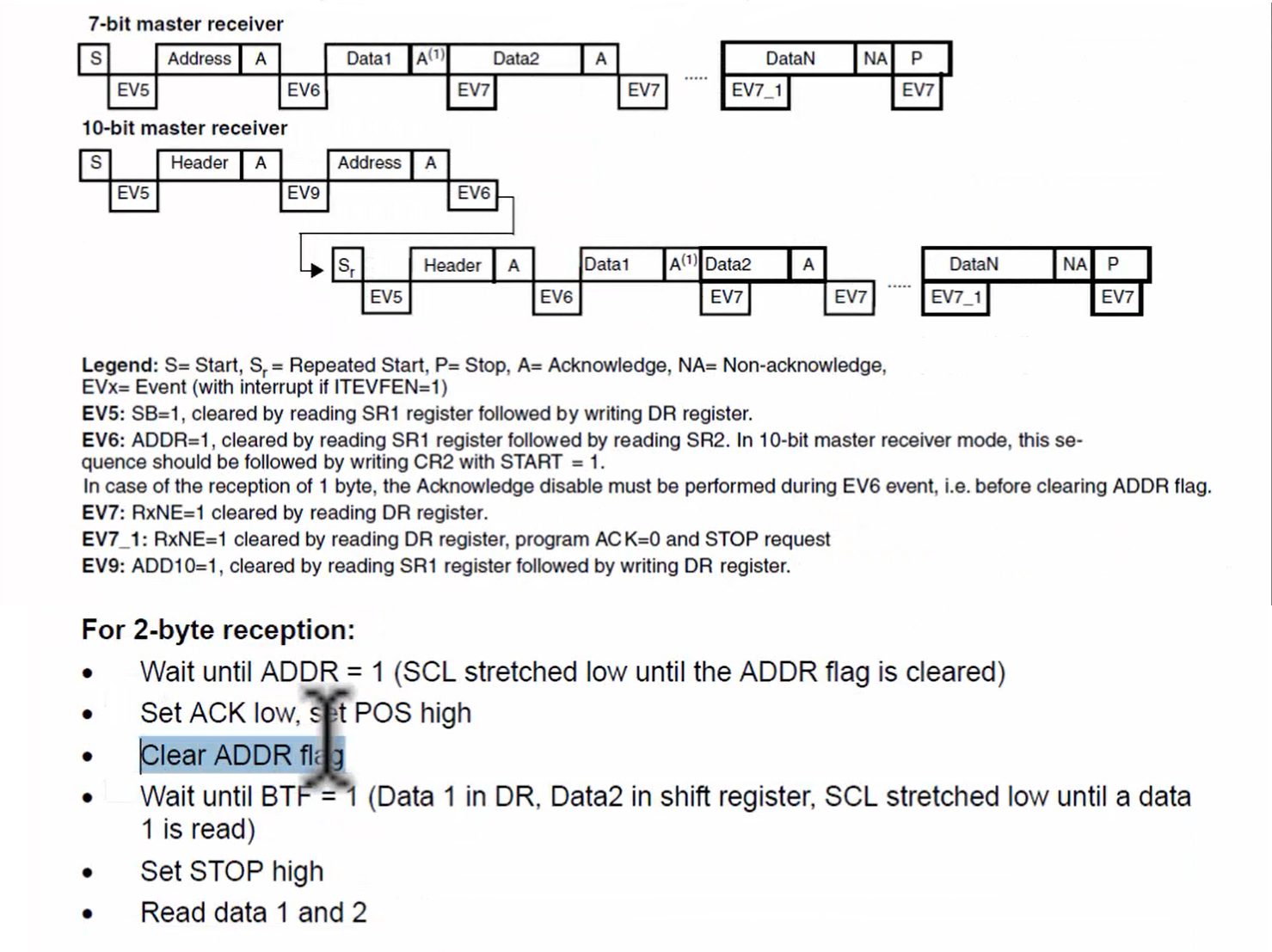
Look at the transfer sequence diagram for a master receiver in Figure 9. Here they are telling us to set the stop bit after clearing the ADDR flag.
Now let’s make the changes to the driver code, as shown in Figure 10.
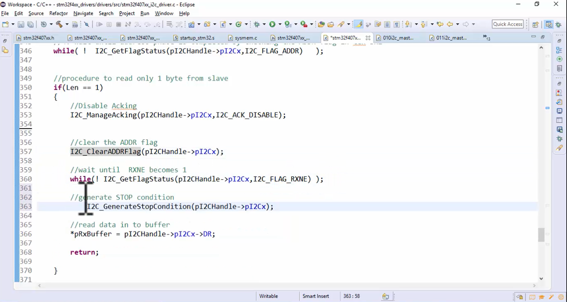
Steps to be followed to check whether the changed code works or not:
- Compile the code.
- Program the board.
- Reset both the boards.
- Capture the result by pressing the start button (Figure 11).
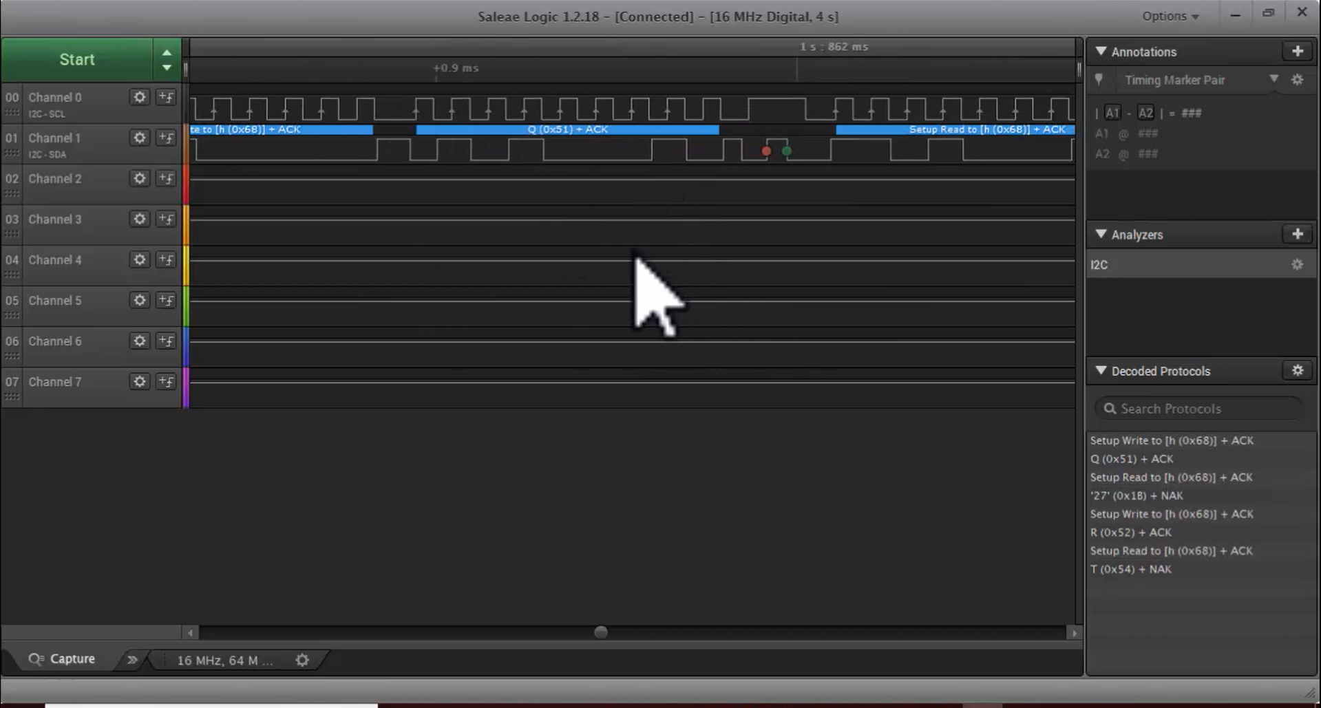
- Observe Figure 11. In the write phase, the master sends the command code 0x51.
- After that master generates the read transaction, and for that transaction, the slave is replied. 27 is the reply from the slave, which you can see in Figure 11.
- After receiving 27, the master sent NACK.
- Since we are interested in only one byte, the stop is generated after receiving one byte.
- Next, the master again generated the write phase, and you can see in Figure 12 that now the master sent command code 0x52. Then the master generated the stop condition.
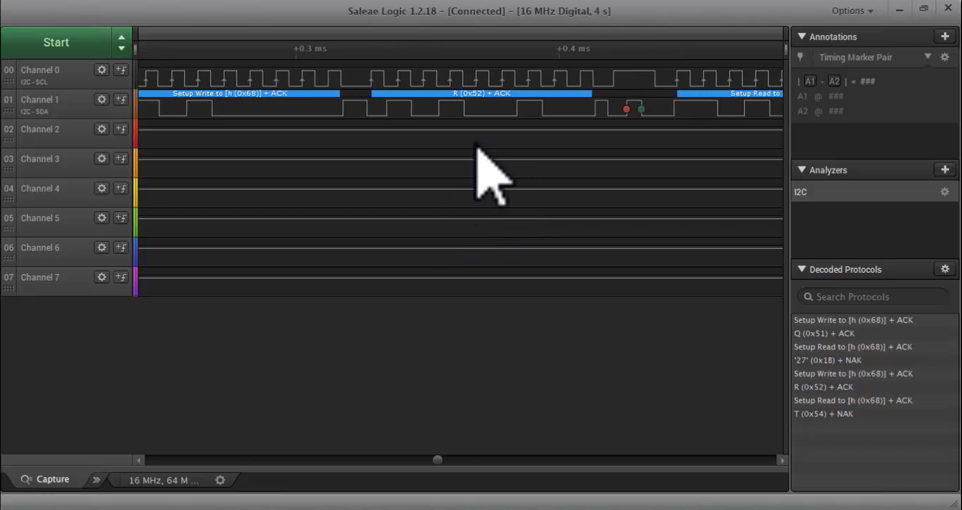
- After that, the master again generated the read transaction, as shown in Figure 13.
- After the start condition generation, the master starts receiving the byte from the slave, and the master receives 1-byte that is T, as shown in Figure 13.
- After receiving 1-byte, the master sent NACK, which is wrong because we should receive 27 bytes.
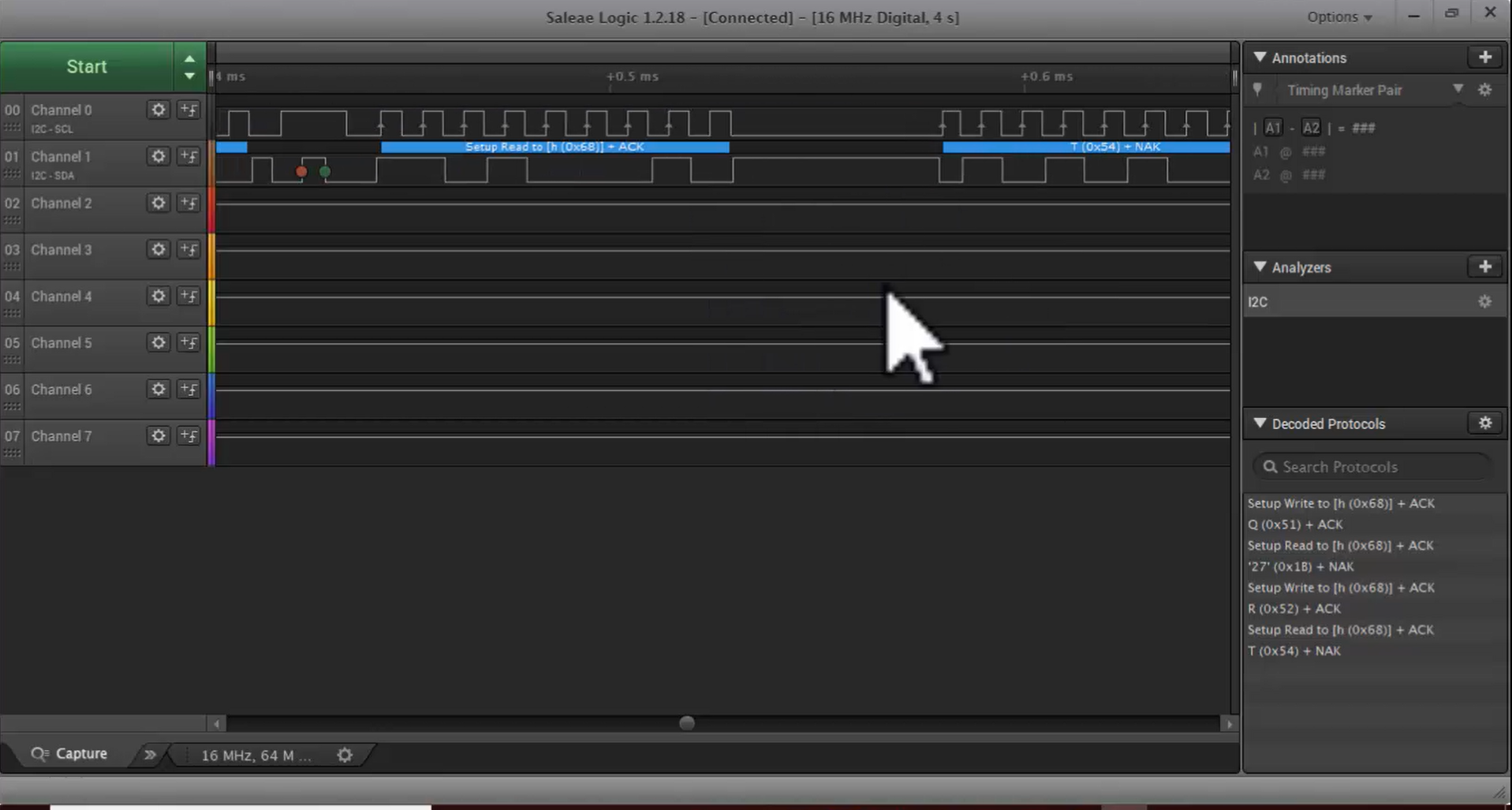
- Here the master didn’t ACK the slave. It only received T. Because, in the Arduino sketch, the data which is being sent is the string shown in Figure 14.
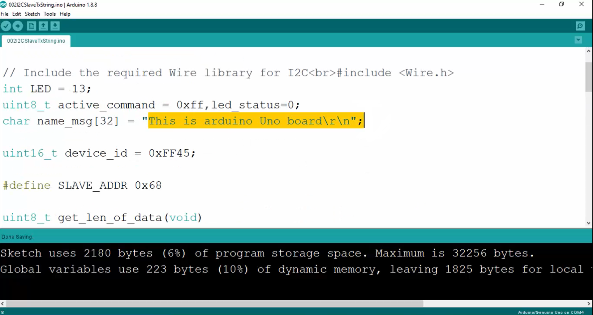
- The slave sent the first character T, but the problem is the master didn’t send the ACK for the received byte.
- Now you have to debug the code to determine why the master code is not sending the ACK.
- To debug the code, go to the debug perspective and make sure that current debugging is off. Click on the terminate button to make the debugging off.
- Then go to breakpoints, and if any breakpoints, then remove all the breakpoints as shown in Figure 15.
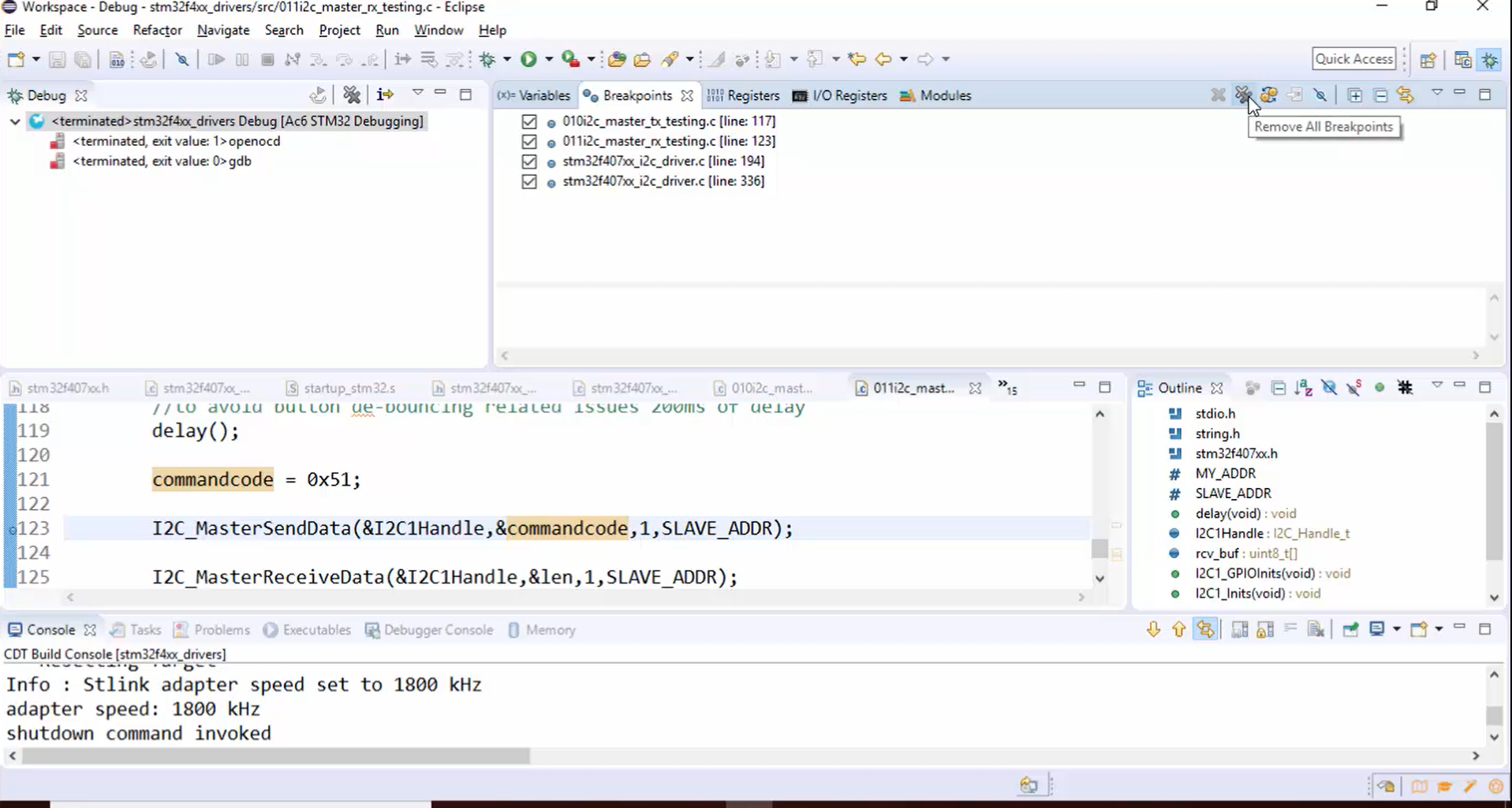
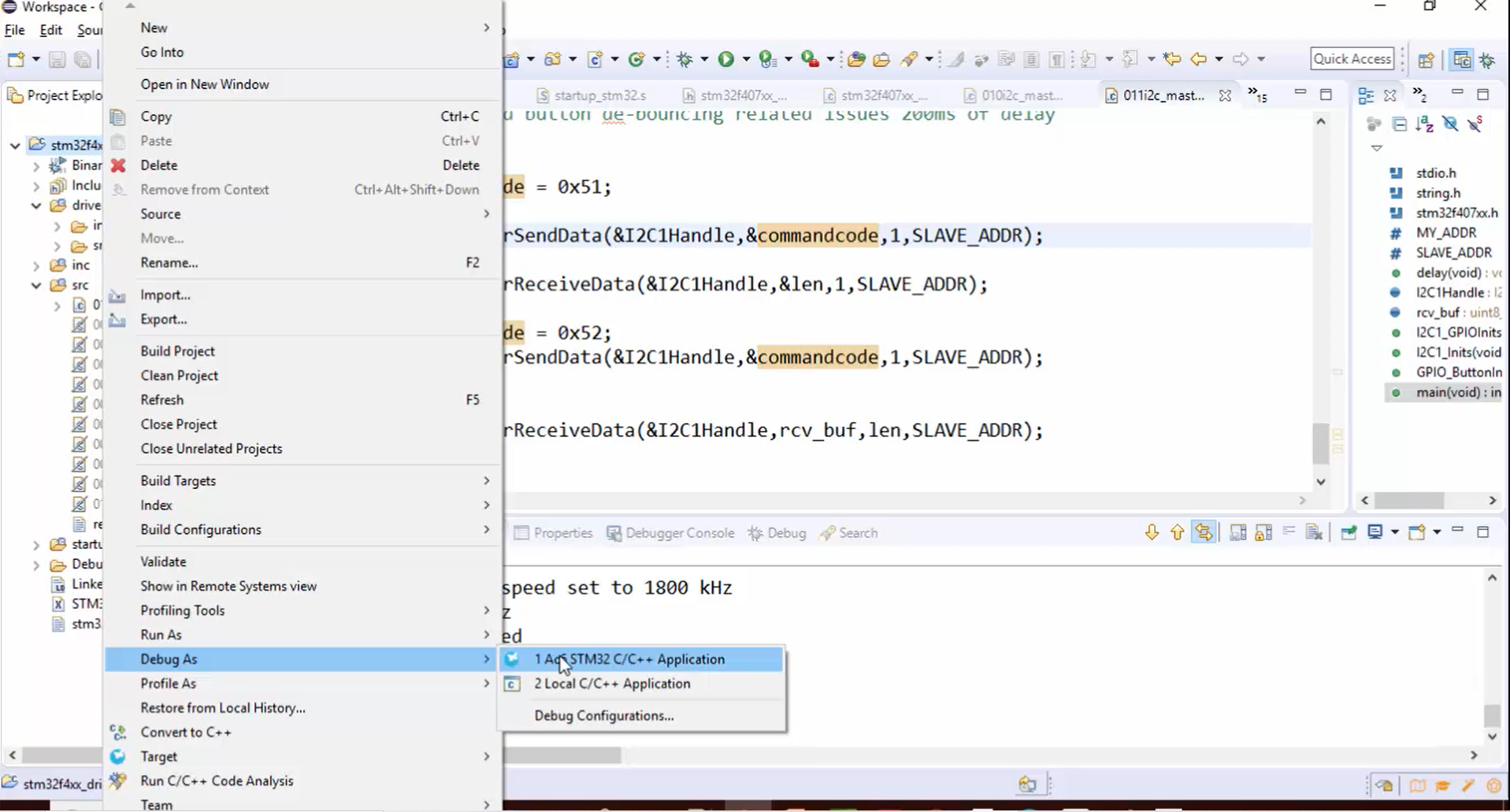
- When you have set many breakpoints, the IDE will crash for some time. So, it is better to remove all breakpoints. Then go to the C and C++ perspective and after that, right-click and go to debug as (Figure 16).
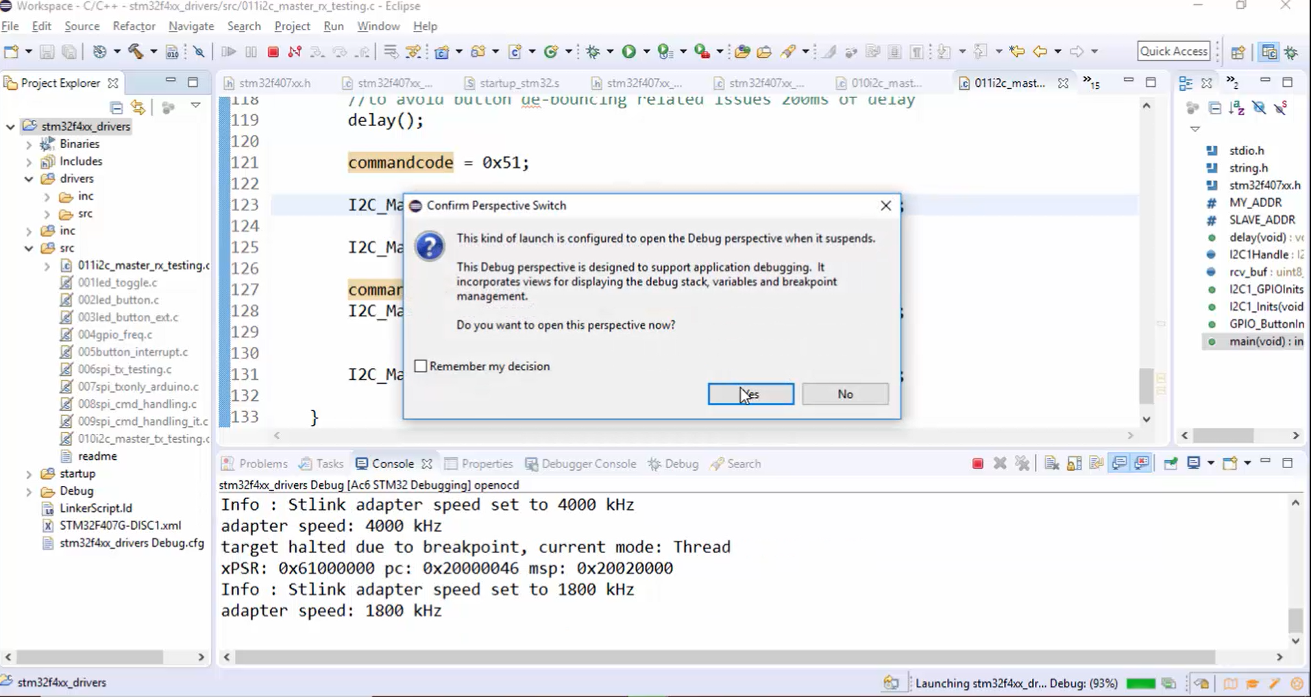
- Launch the debugger by clicking on yes, as shown in Figure 17.
Now the problem is the master is not sending the ACK. That means the troubleshooting point would be checking whether the ACK bit is enabled or not in the master.
In the I2C init function, the ACK is enabled (Figure 18), but we should understand whether it is really affecting the control register or not. That means in the control register, you have to check whether the ACK is really enabled or not.
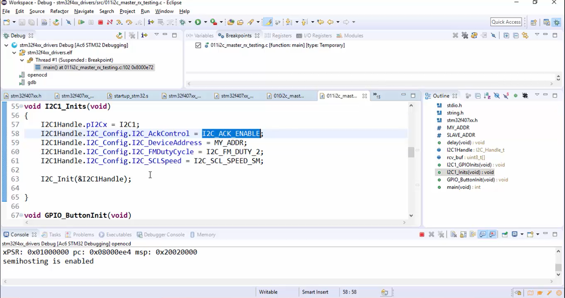
- Figure 19 shows the code for enabling the ACK in the CR1 register. Let’s keep the breakpoint here as in Figure 19.
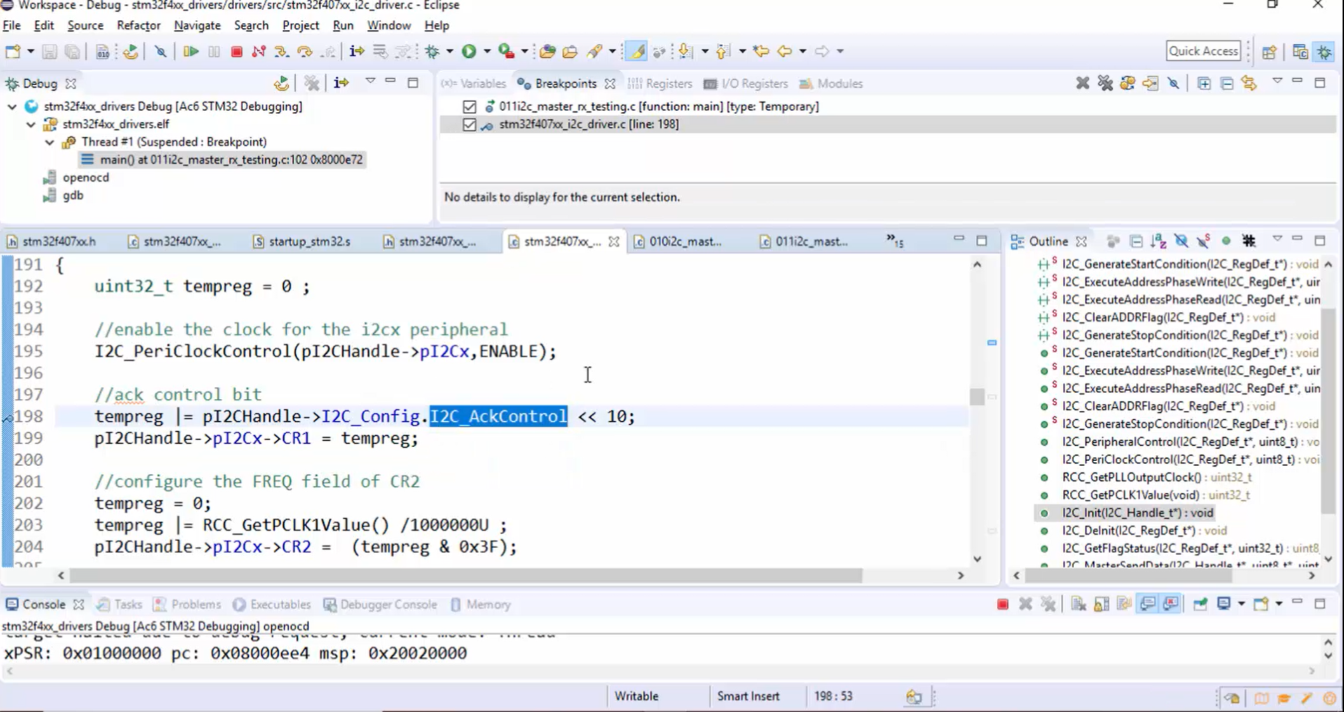
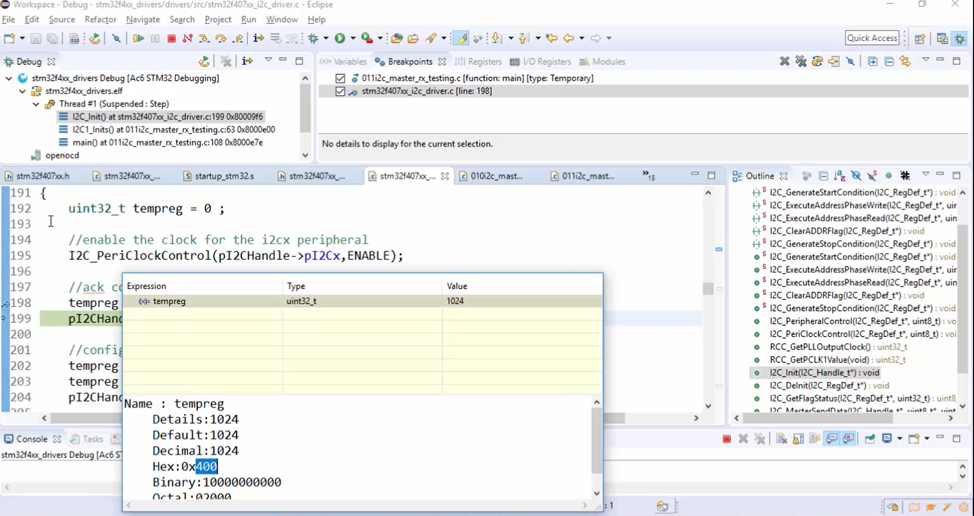
- Hit the run. The control has reached the breakpoint, then let’s do a single step and analyze the tempreg value. Now the tempreg value or the 10th bit is set, as shown in Figure 20.
- Check whether the CR1 will get affected or not: Go to the I/O registers, select I2C, then open I2C1. In Figure 21, you can see that the CR1 is currently 00.
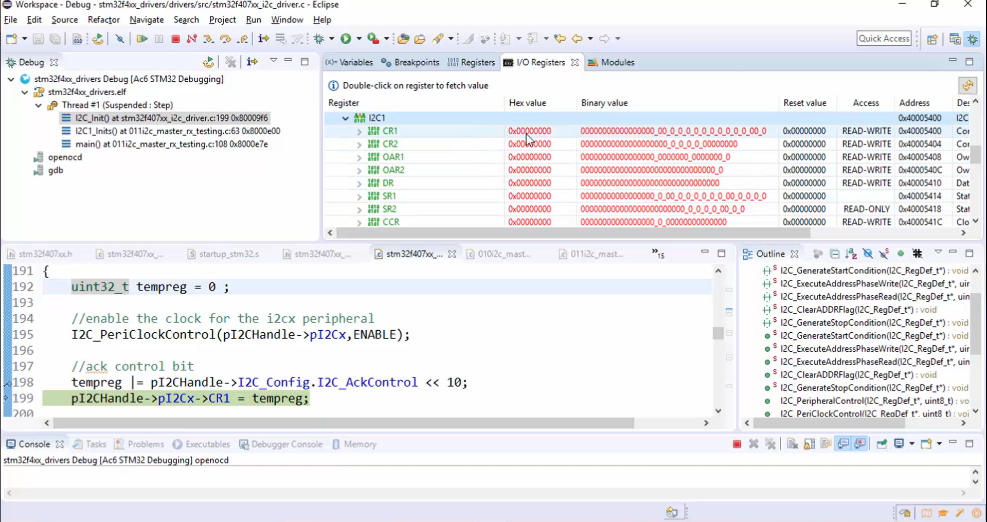
If everything is fine, then in the CR1 register, the ACK field must be one after executing line 199. Let’s do a step over. Then update the CR1 register by double-tapping it.
In Figure 22, you can see that the ACK bit is not set. That’s why the master is sending NACK.
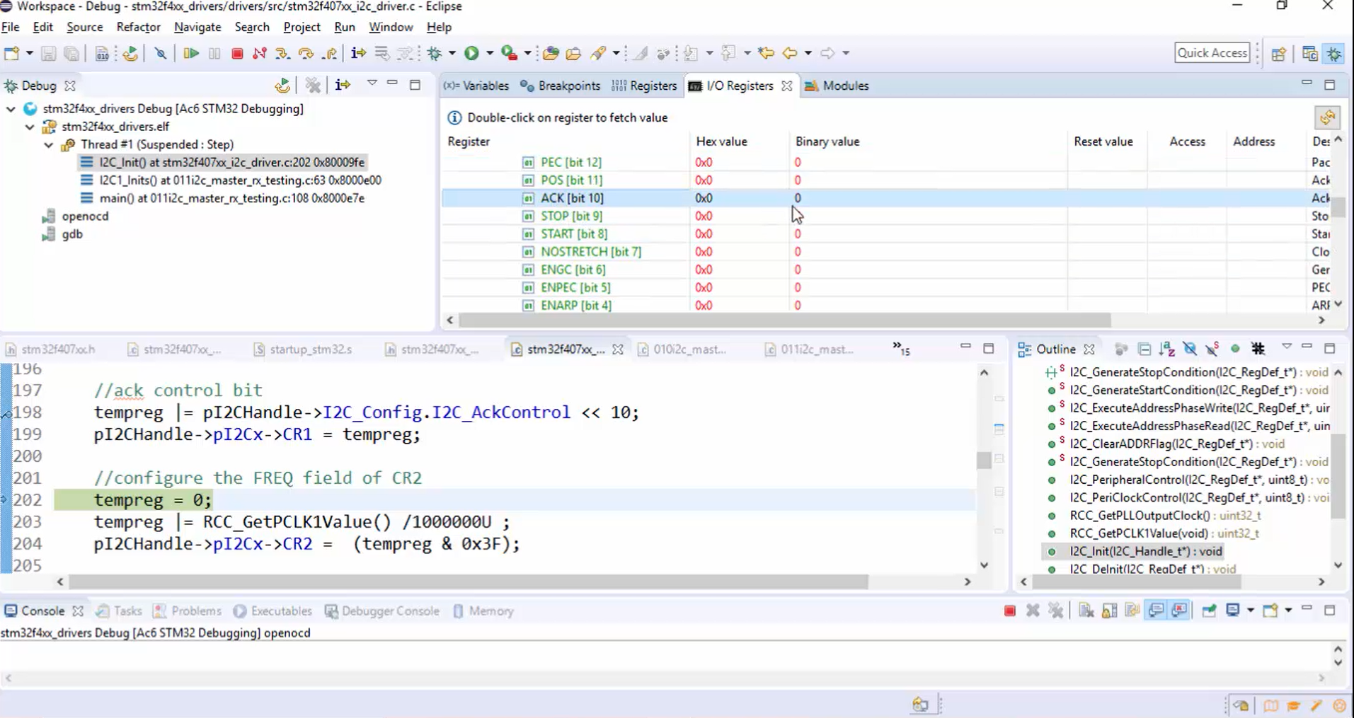
Now why this is happening even though the 10th bit of tempreg is indeed set to 1. To resolve this problem, you have to understand the ACK bit in the control register completely.
Observe Figure 23. Here the ACK bit explanation says that ACK bit is set and cleared by the software and cleared by the hardware when PE=0.
Look at Figure 24. In our application, the PE=0. It is impossible to make ACK=1 when PE=0. The ACK bit will become one only when you set the PE bit.

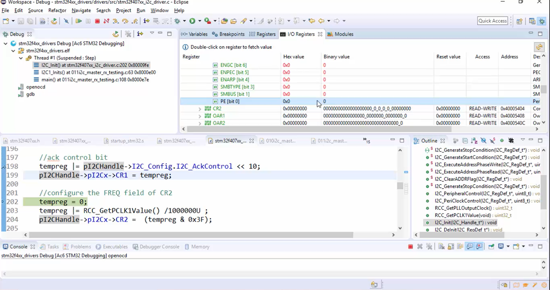
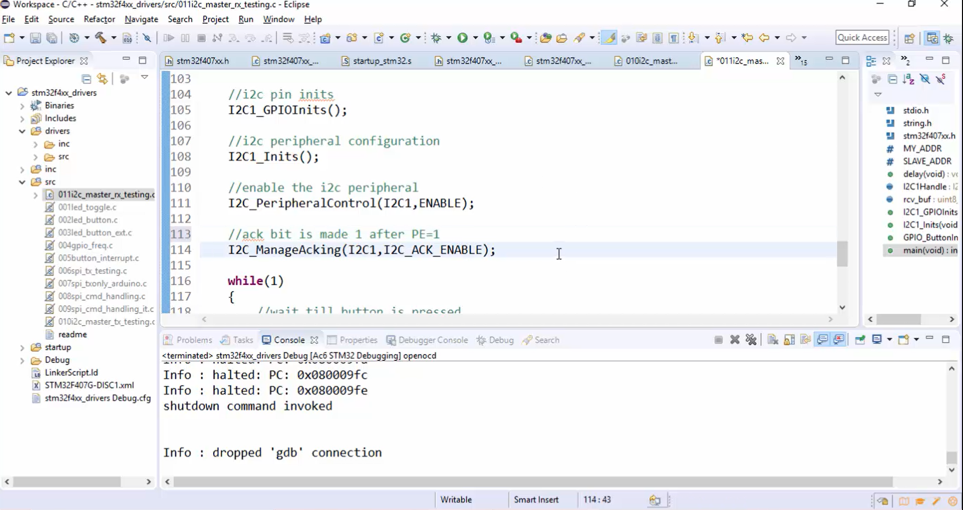
Go back to the project and make the necessary changes to the code as follows:
- Enable the ACK bit after PE=1, as shown in Figure 25.
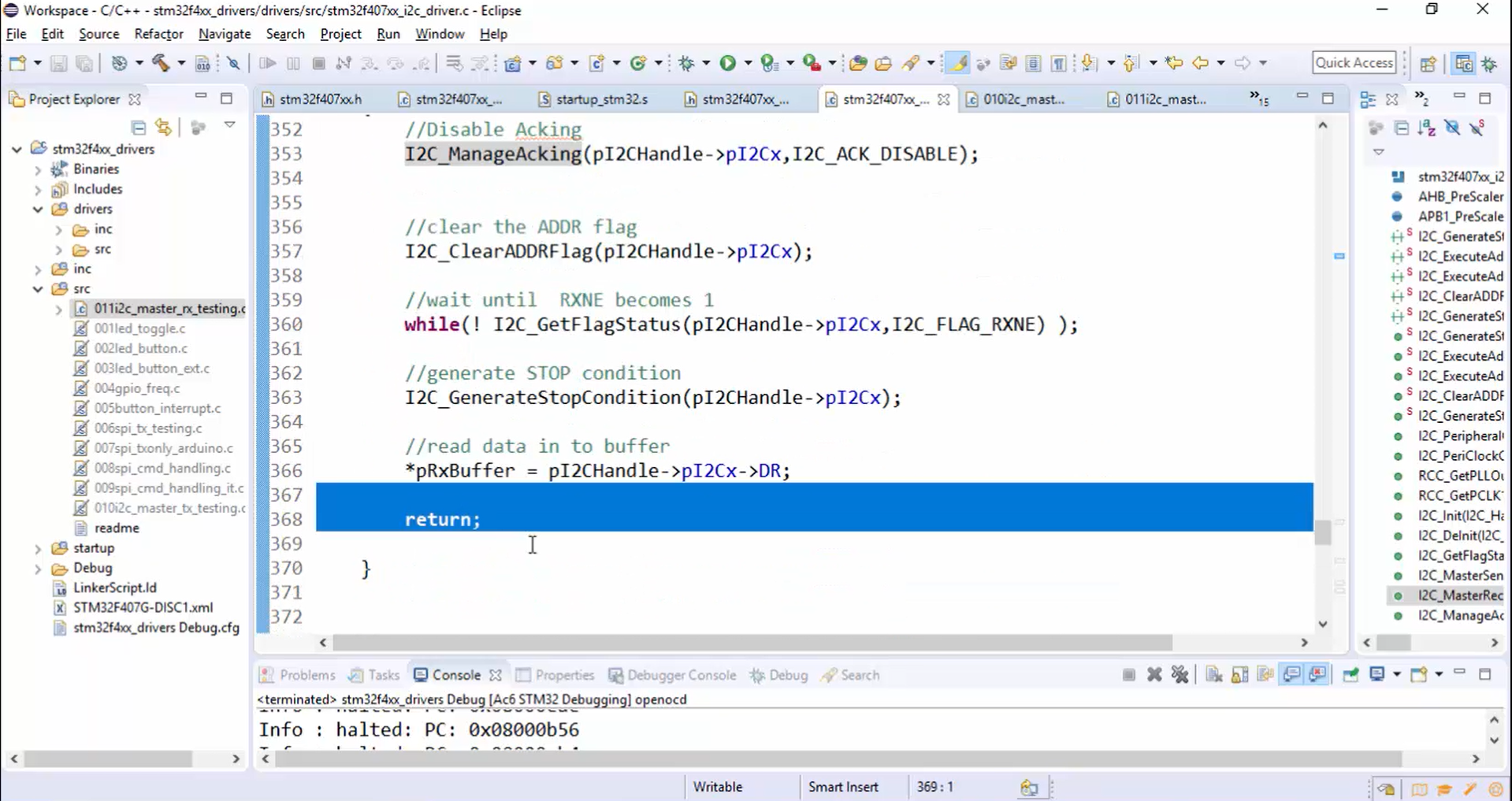
- Make sure that you have re-enabled (Figure 26) the ACK bit before leaving the master receive data API.
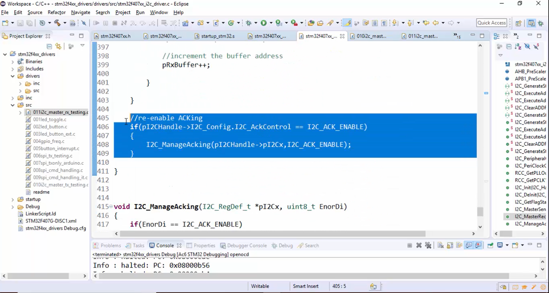
- There is a return statement at the end of the MasterReceiveData API, which makes the program control to return before re-enabling the ACK. Therefore, remove the return statement shown in Figure 27.
- Now compile the code.
- Program the board.
- Reset both the boards.
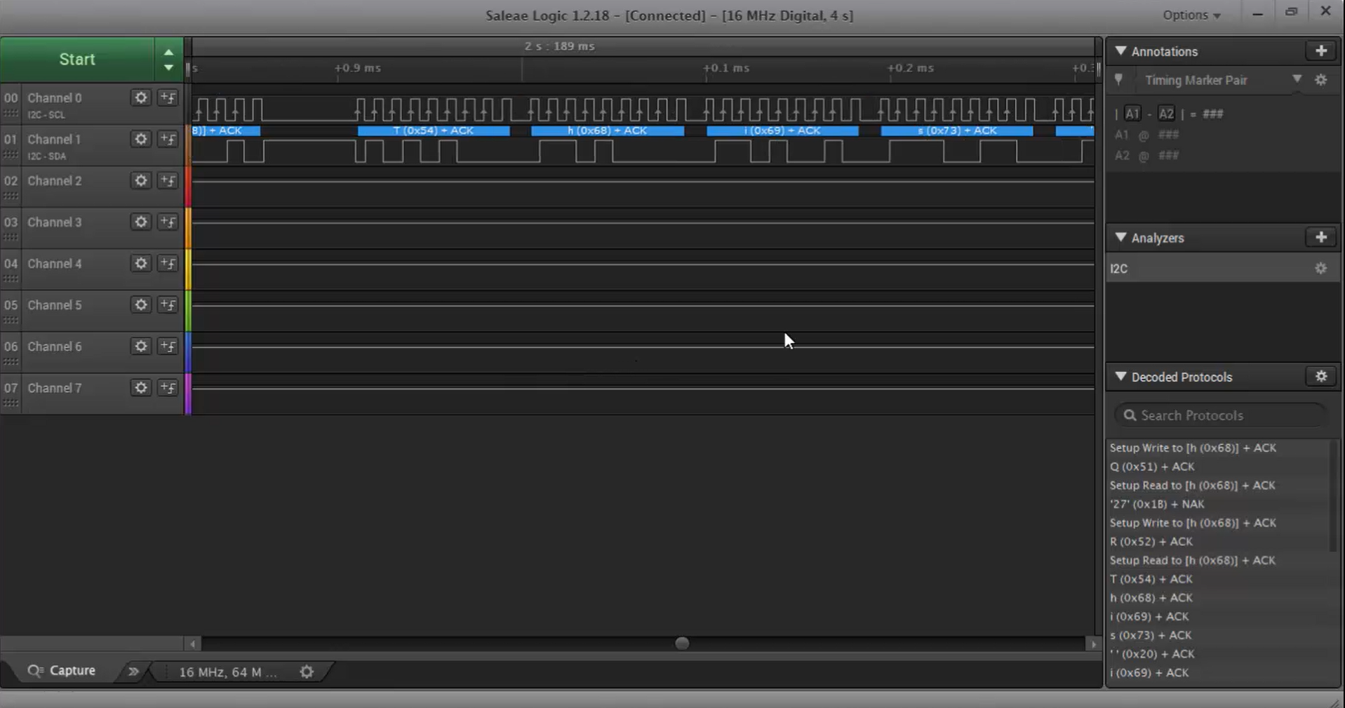
- Capture the logic analyzer results by pressing the user button. In Figure 28, you can observe all the bytes which are being received from the slave. The last two characters are \r and \n (Figure 29), which is there in the string sent by the Arduino sketch shown in Figure 14.
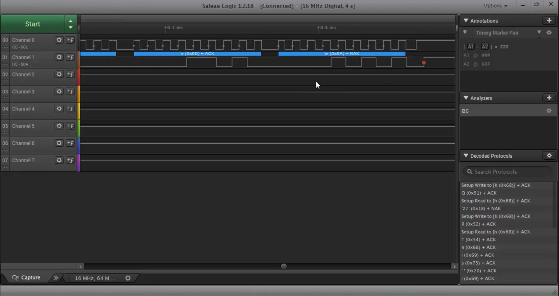
- The stop is generated, and both the lines are released, as shown in Figure 29.
Let’s continue in the following article. Click Here.
FastBit Embedded Brain Academy Courses,
Click here: https://fastbitlab.com/course1

