I2C pull up resistance, rise time and bus capacitance discussion
Before doing the exercises on I2C, we have to cover some important concepts related to I2C communication. They are as follows:
- Calculation of the right pull-up resistance for the application.
- Calculation of rise time.
- Calculation of bus capacitance.
These are very important discussions, and it will help achieve successful communication between devices using the I2C protocol.
Calculation of the right pull up resistance for the application:
There are two equations in order to calculate the pull-up resistor, as shown in Figure 1.

The first equation gives the minimum value of the pull-up resistance required for the application. The pull-up resistance minimum value is a function of the VCC or VDD, which is the main supply for the microcontroller, VOL (max), and IOL.
Basically,
RP (min) = V/I
Where VOL means low-level output voltage. Ideally, VOL will be zero, the low-level output voltage is 0, and the high-level output voltage means VCC. But in I2C specification, voltage up to 0.4V is considered as low-level output voltage.
VOL value is given in the I2C specification. Look at Figure 2, here it is given that when VDD > 2, the low-level output voltage is equal to 0.4, and the IOL value can be considered as 3mA.
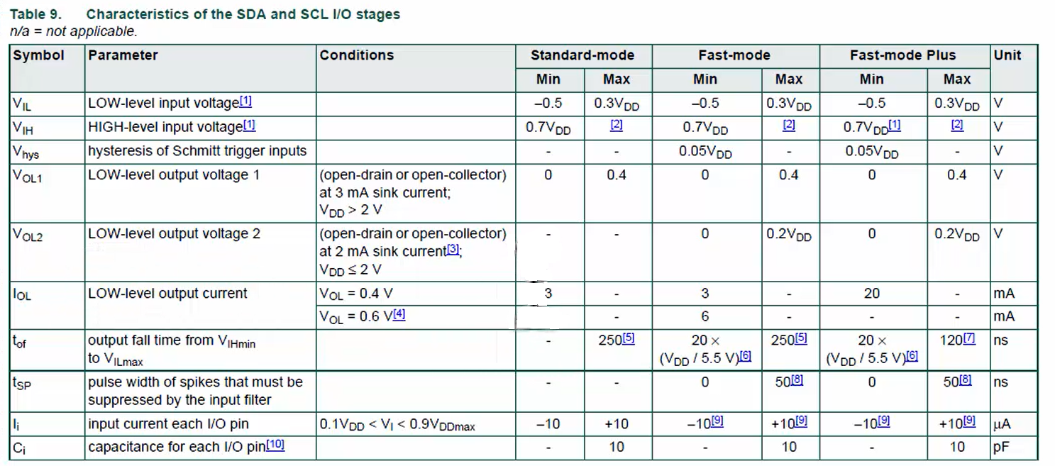
Now, substitute all these values into equation 1 of Figure 1 to calculate the minimum value of the pull-up resistors.
For example, let’s consider the scenario (Figure 3) where the signal, either SDA or SCL, is going from high to low.

Consider that High is VCC and low is 0, and the VOL is somewhere near the 0. When SCL or SDA goes low, then the transistor in Figure 3 will conduct, and the current IOL flows through it. Therefore, the resistance of the RPU can be easily calculated using the formula:

Solve this equation to get the minimum value of RPU that is pull-up register.
Use the second equation in Figure 1 to calculate the maximum value. The maximum pull-up resistance is the function of the maximum rise time (tr). This is a very important equation because it is a function of rise time and bus capacity. Where tr means rise time of both SDA and SCL signals and Cb means capacitive load for each bus line.
Rise time (tr):
Consider the waveform in Figure 4. It can be either SDA or SCL. Now, look at the tr. It is the gap between 30% of the voltage level to 70% of the voltage level.
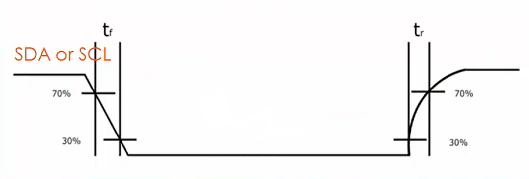
Therefore, the rise time or tr is defined as the amount of time taken by the rising edge to reach 70% amplitude from 30% amplitude for either SDA or SCL.
Ideally, the tr must be zero. If you consider the scenario in Figure 4, the signal is rising from low to high by taking a significant amount of time that time is denoted by tr or rise time. The rise time should not be high because if it is too high, it will cause a problem during I2C communication. The value of the pull-up resistance and the bus capacitance influence the tr timing. The tr is proportional to the RC time constant. Therefore, an increase in the value of pull-up resistance, and bus capacitance increases tr.
tr increasing means something is becoming a hurdle for SDA/SCL line to rise to VCC level or someone is resisting the signal to rise to VCC. The hurdle is RC time constant. Where R is the value of the pull-up register, and C is bus capacitance. The hurdle faced by the signal to reach its 70% is a problem here.
I2C specification is very serious about this problem, and some maximum limit for tr is given to overcome this problem. The maximum limit of tr is 1000 nanoseconds for standard mode. While using standard mode, the tr of the signal (either SDA or SCL) should not be more than 1 microsecond or 1000 nanoseconds.
I2C specification cares about tr value and have to respect it while calculating the pull-up register value. A higher value of pull-up registers (weak pull-ups) increases the tr value (not acceptable if tr crosses max limit mentioned in the spec). The pull-up register with a very high value will prevent the signal from reaching 70% of the VDD, as shown in Figure 5.
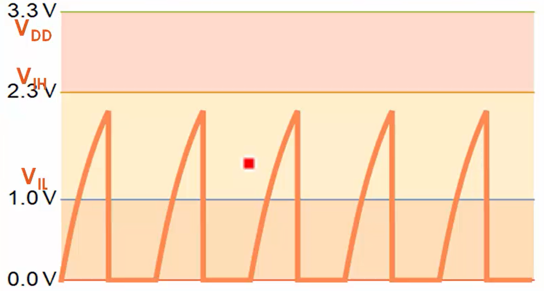
If it does not reach 70% of the VDD that is 2.3V in this case (Figure 5), then the signal is not considered as high, and the slave will receive some garbage values, or I2C communication will fail. If the signal fails to reach at least 70% of the VCC or VDD in the oscilloscope, as shown in Figure 5, you should conclude that the RC time constant is very high.
To solve this problem, either bring down the register or R-value or decrease the bus capacitance. You can also write RpCb instead of RC, where Rp stands for pull-up resistance and Cb is the bus capacitance.
The lower value of pull-up registers (strong pull-ups) decreases tr value, but they also lead to higher current consumption because when the resistance becomes very low, more current flows across the transistor resulting in more current consumption.
The higher power consumption is bad for power-aware or low power applications. That’s why you have to select one of the values between RP (min) and RP (max) as the value of pull-up resistance. Here you will get the RP (min) and RP (max) values by solving the equations in Figure 1.
Bus capacitance (Cb):
Capacitance means that the voltage level on the signal line (data or clock) cannot change instantaneously.
For example, consider the circuit or bus in Figure 6. There we have SCL and SDA line and connected 4 devices. Even though you don’t connect any capacitor in the circuit, the accidental capacitor called parasitic capacitor resists the flow and becomes a hurdle for the signal to rise from zero to a high state. So, while calculating the pull-up resistance, the value of the bus capacitance also must be taken into account, as in the case of RP (max) calculation.
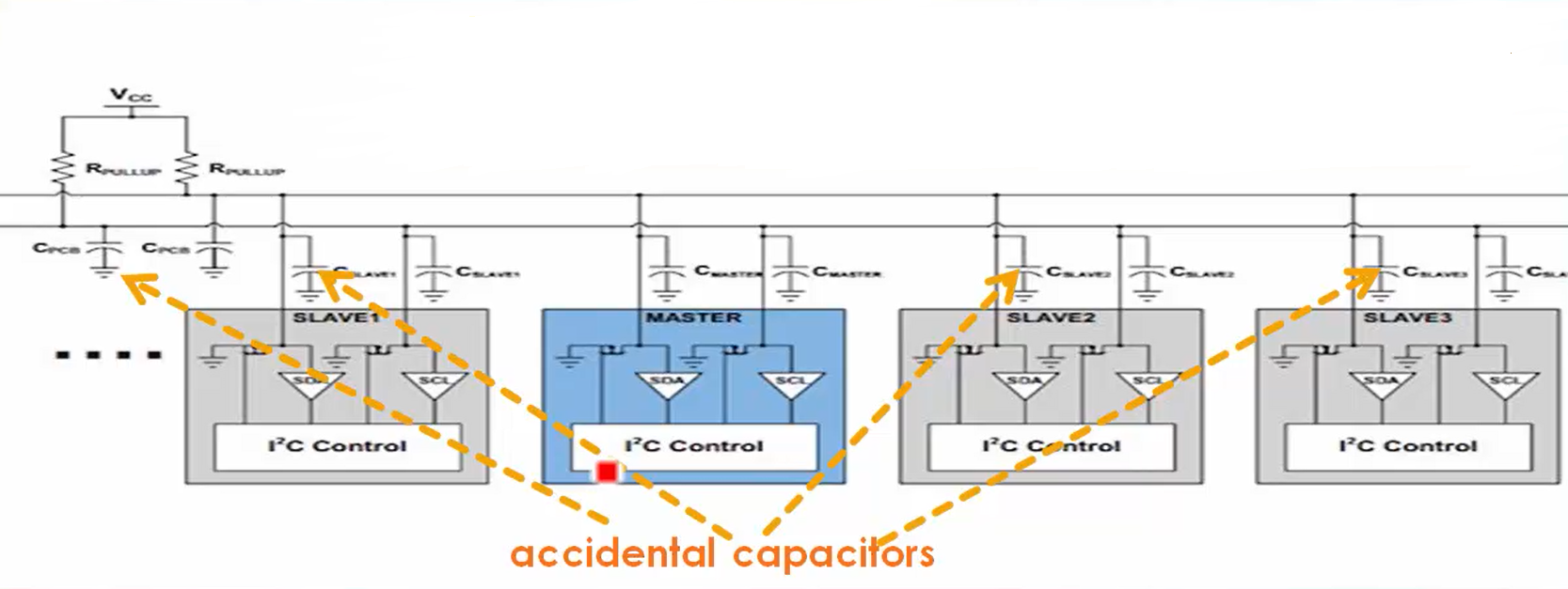
- Bus capacitance is a collection of individual pin capacitance with respect to ground, the capacitance between the SDA and SCL, parasitic capacitance, capacitance added by the devices hanging on the bus, bus length (wire), dielectric material, etc. All these are reasons for accidental capacitors in the I2C bus.
Remember that, as the bus length or wire length increases, the capacitance also increases, and more devices on the bus means more pin capacitance has been added to the bus.
- Bus capacitance limits how long your I2C wiring can be and how many devices you can connect on the bus because there is a limit for bus capacitance in the specification.
Figure 7 shows a specification value for tr (rise time) of both SDA and SCL signals, it should not cross 1000 nanoseconds, and the maximum bus capacitance for standard mode and fast mode is 400pF. Therefore, the overall bus capacitance of the application should not cross 400pF.
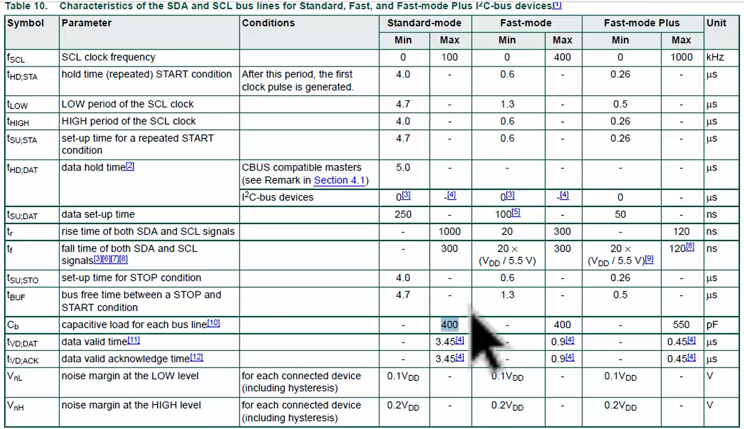
- For maximum allowed bus capacitance, check the specification: Consider an exercise, for fast-mode I2C communication with the following parameters, calculate the pull-up register value. Cb = 150pF, VCC = 3.3V.
Remember that the bus capacitance can be calculated by using capacitance measurement tools or multi-meter, or some advanced tools. But you can model a bus to calculate the approximate value of the bus capacitance.
Now consider that you have an I2C bus with 4 devices connected, as shown in Figure 6. Each device will add its own pin capacitance to the bus. Let’s consider it as 10pF for each device. Since it has 4 devices, approximately 40pF of bus capacitance will be added to the bus from the devices.
- Another 100pF of capacitance is added by considering the length of the wires like SCL or SDA and other factors like PCB wirings, dielectric mediums, etc. Therefore, in this case, total capacitance has to be adjusted to 150pF or even less or more than that. The pin capacitance of the device is mentioned in the specification of the I2C device.
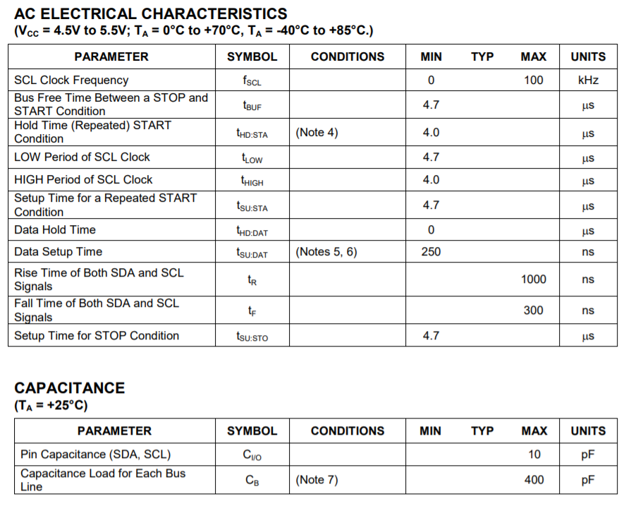
For example, Check the datasheet DS1307 I2C based Real-Time-Clock shown in Figure 8. It will give you lots of information about I2C communication and the recommended settings information.
Look at Figure 8. This device can communicate only in standard mode since the maximum serial clock frequency is 100kHz. The pin capacitance for the SDA and SCL are given in the capacitance table, which is 10pF. Therefore, each device will add a 10pF of capacitance to the bus.
Now let’s solve the given exercise,
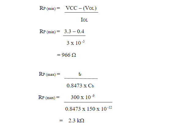
If you select RP = 2.2 kΩ, then it is a good value. It prevents higher current consumption and also takes care of the rise time requirements. But if you blindly use 22 kΩ, then it would cause problems for the Trise requirements. The Trise may go out of 300 nanoseconds if the bus capacitance is too high.
No need to use the external pull-up registers for this exercise because there are a few devices connected on the bus, and the length of the wire is also very short. Instead, the exercises can be tested with an internal pull-up resistance of 40 kΩ.
The correct value of the pull-up register must be calculated by considering the Trise and bus capacitance while developing a product based on the I2C protocol. The Trise timing for the I2C communication must be configured in the I2C driver by programming the Trise register of the I2C register shown in Figure 9.

In the following article, let’s see I2C rise time calculation.
FastBit Embedded Brain Academy Courses
Click here: https://fastbitlab.com/course1


