SPI CPOL and CPHA discussion
In this article, let’s discuss the SPI communication formats. During SPI communication, receive and transmit operations are performed simultaneously.
The serial clock (SCK) synchronizes the shifting and sampling of the information on the data lines. The communication format depends on the clock phase(CPHA), the clock polarity(CPOL), and the data frame format.
To be able to communicate together, the master and slave devices must follow the same communication format. Otherwise, data communication will not be successful. Because the master may read the invalid data from the slave or slave may receive some corrupted data etc. So the communication formats must be the same in both master and slave devices.
The data format is straightforward to understand. The data format can be a 16-bit data format or 8-bit data format. By default, master and slave communicate over the 8-bit data format.
Clock polarity (CPOL):
The CPOL bit controls the idle state value of the clock when no data is transferred. This bit affects both master and slave modes. If CPOL is reset, the SCK pin has a low-level idle state. If CPOL is set, the SCK pin has a high-level idle state. So, in the SPI control register, there is a bit called CPOL, and you can make that pin as either a 0 or 1.

From Figure 1. When CPOL=0, the clock starts from 0 or low level and then it toggles. Here the idle state is 0, which is at the end of the clock cycle.
Idle state means when there is no communication between master and slave the clock line or serial clock pin will be at 0 or low level. When CPOL=1, the clock starts from a high level or 1. So, there is a transition from high to low state. Here the idle state is 1. That means when there is no communication between the master and slave, the status of the serial clock pin is high. Depending on the application requirements, one can select either CPOL=0 or CPOL=1. By default, the clock polarity is 0.
Clock phase (CPHA):
It decides the clock phase. CPHA controls at which clock edge that is the 1st or 2nd edge of SCLK, the slave should sample the data. The combination of CPOL (clock polarity) and CPHA (clock phase) bits selects the data capture clock edge.
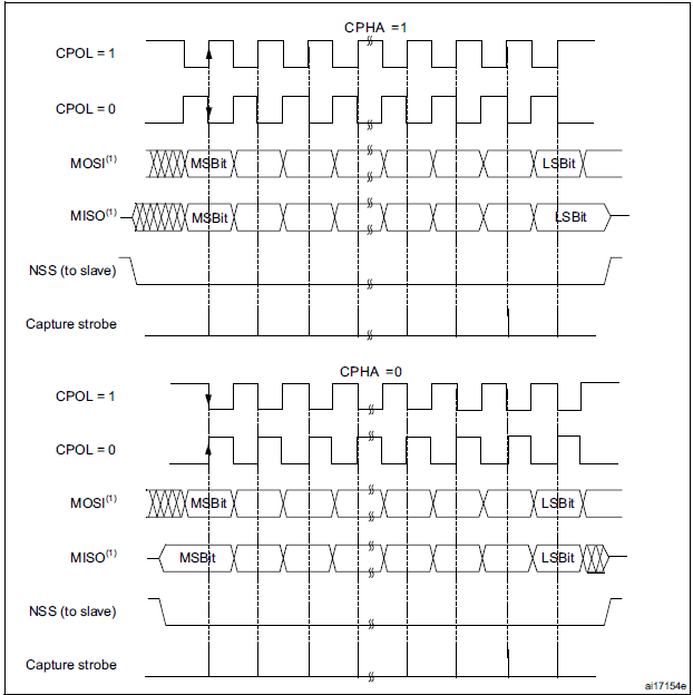
From Figure 2. If the CPHA bit is set, that is CPHA=1, the second edge on the SCK pin captures the first data bit transacted(falling edge if the CPOL bit is reset, rising edge if the CPOL bit is set). Data are latched on each occurrence of this clock transition type.
If the CPHA bit is reset, that is CPHA=0, the first edge on the SCK pin captures the first data bit transacted (falling edge if the CPOL bit is set, rising side if the CPOL bit is reset). Data are latched on each occurrence of this clock transition type. But for all standard operations by default CPHA=0 and CPOL=0. Based on these CPHA and CPOL combinations, there are four different SPI modes. That is,
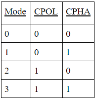
If CPHA=1, data will be sampled on the trailing edge of the clock. If CPHA=0, data will be sampled on the leading edge of the clock.
The last one is the data frame format. The data frame size is chosen by the DS bits in the SPIx_DR register. It can be set from 4-bit up to 16-bit length, and the setting applies for both transmission and reception. During communication, only bits within the data frame are clocked and transferred.
From Figure 3. The master is in transmit mode, and the slave is in receive mode. The MOSI of the master connects to the MOSI of the slave. And both the MISO lines are disconnected.
In all of the above communications, the NSS pin is optional because only one slave considered.
FastBit Embedded Brain Academy Courses
Click here: https://fastbitlab.com/course1

