Configuring GPIO pins for SPI functionality
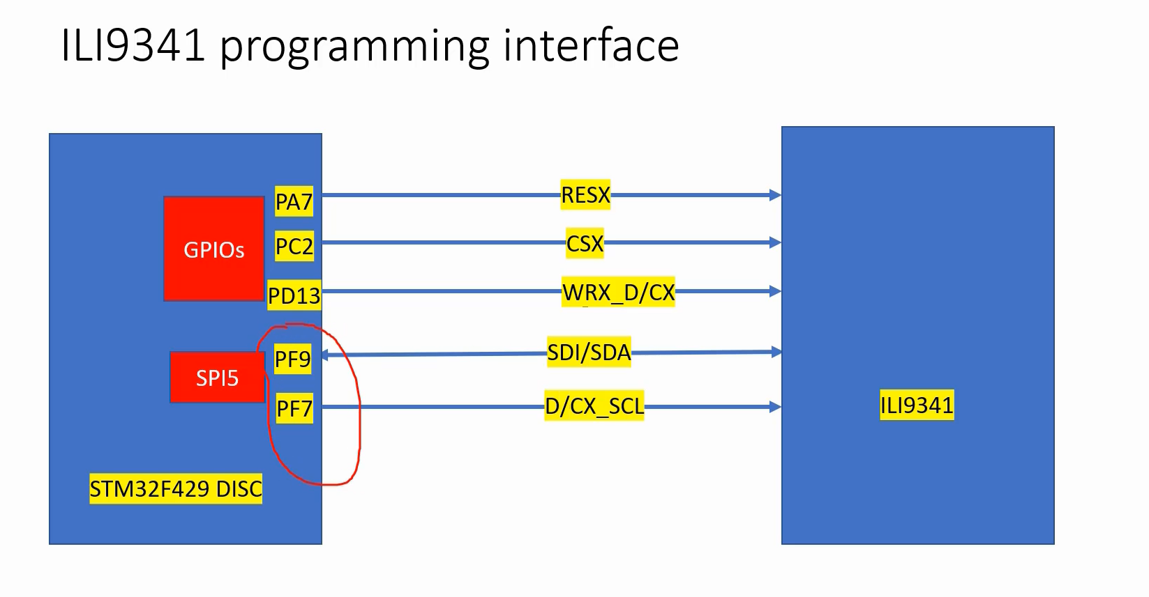
In this diagram, you can see that we have PF9 and PF7 pins that need to be configured for SPI functionality. The SPI peripheral being used is SPI5.
For that, you have to follow these steps.
Configuring GPIO pins for SPI functionality
- Configure the GPIO pin to alternate function mode.
Because, the pin is now used for an alternate function, that is SPI.
- Configure the alternate function mode number in the alternate function register (you can get the alternate function mode number from MCU datasheet).
- For SPI communication, No pull up or pull down resistors are required.
That’s why we will not be using the pin in the open drain setting. You can just use an output type as push-pull.
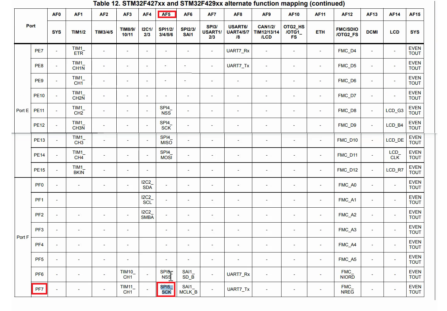
The pins we need to touch are GPIO port F, pin numbers 9 and 7. Refer to the datasheet to identify the alternate functions supported by these pins.
In the STM32F429zi datasheet, navigate to the Pinouts and Pin Description section and locate the appropriate device, which in this case is the STM32F429 as shown in Figure 2. From there, navigate to Port F and specifically to Pin PF7 which can be configured to act as an SPI clock when its alternate function is set to 5. The mode number for this pin should also be set to 5.
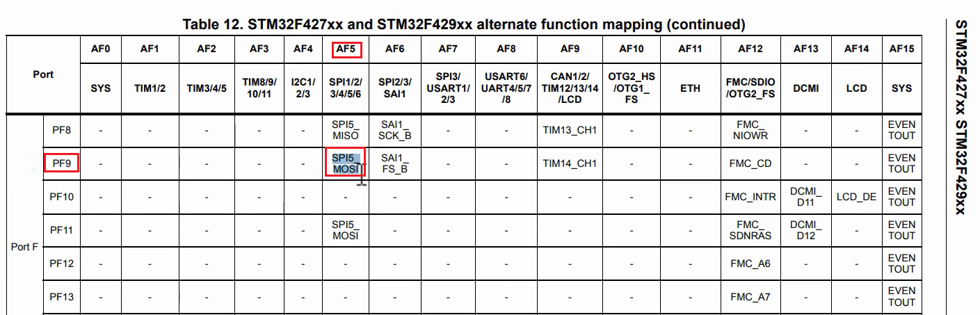
Similarly, Pin PF9 can act as SPI5_MOSI, but only if its alternate function mode is set to 5.
Where to configure this value 5? That you have to do in the alternate function register of the GPIO.
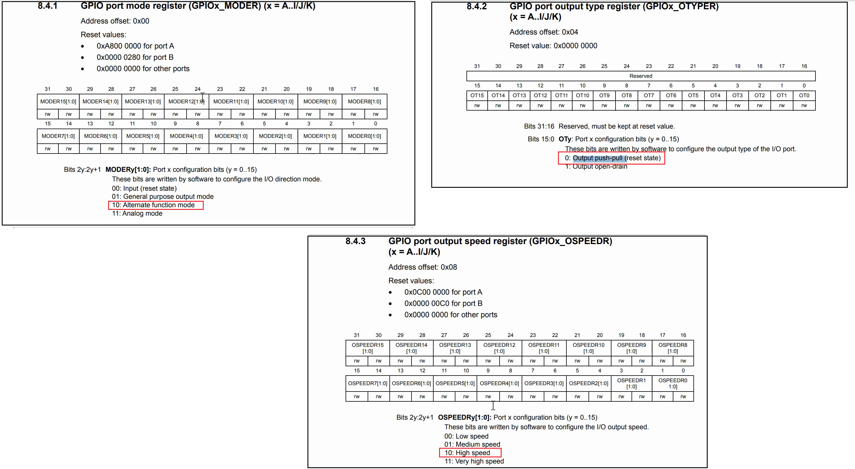
Let’s head to the GPIO registers section. In the Mode register, you need to select the alternate function mode. Next, in the Output Type register, simply choose push-pull. After that, you can select a high speed in the Output Speed register (as shown in Figure 4).
The pull-up, and pull down settings are not required, and then go all the way to GPIO alternate function low register or high register.
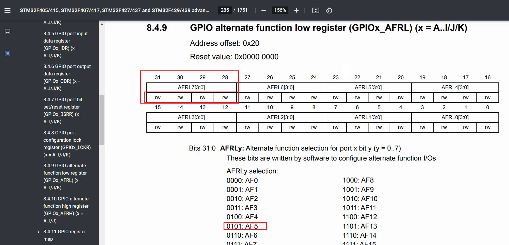
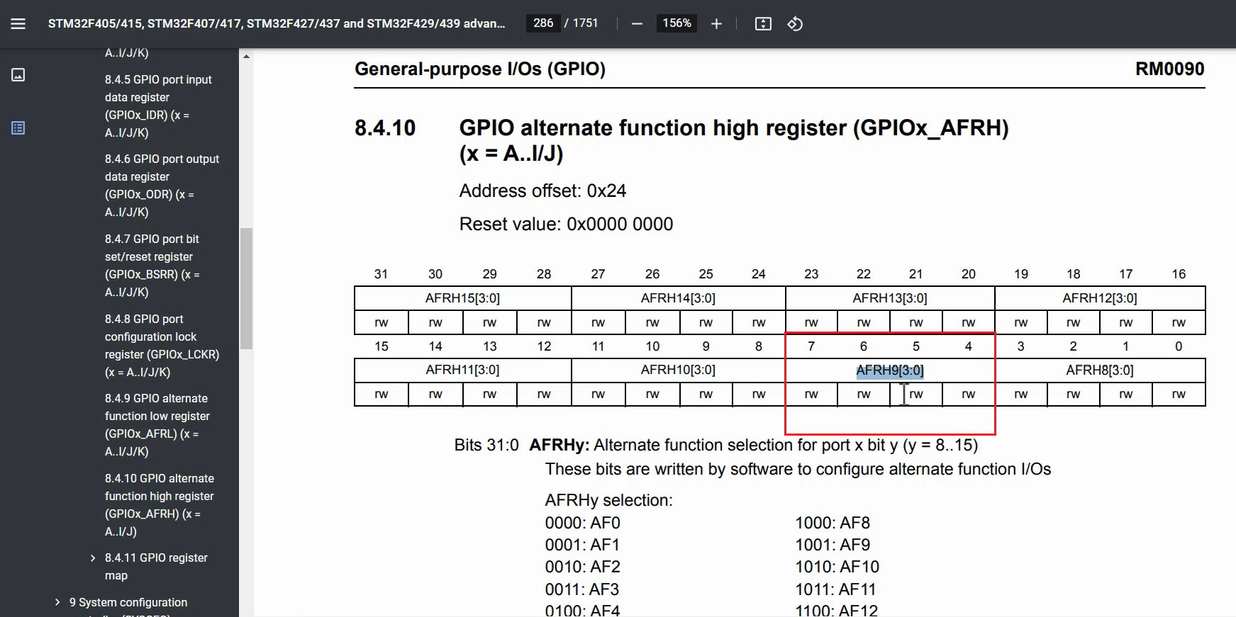
First, we need to configure the alternate function for PF7. Since PF7 is a pin number less than 8, we must configure the function low register. In the low register, each pin takes a 4-bit field.
By using the low register, we can configure the alternate function for 8 pins, ranging from 0 to 7. Therefore, for PF7, which is the 7th pin, we need to configure the appropriate fields(AFRL7 – 0101). Here we have to store the value 5. To achieve this, we can use the REG_SET_VAL macro.
By doing so, we can easily configure the alternate function for PF7.
After that, for PF9, as 9 is greater than 8, you cannot use the low register and must switch to a high register. Therefore, you need to modify the bit fields in the alternate function high register for pin number 9 and store the value 9 there.
Initialize the GPIO pin to SPI functionality
Let’s start with SPI SCL, that is SPI_CLK and the pin is PF7(Figure 7).
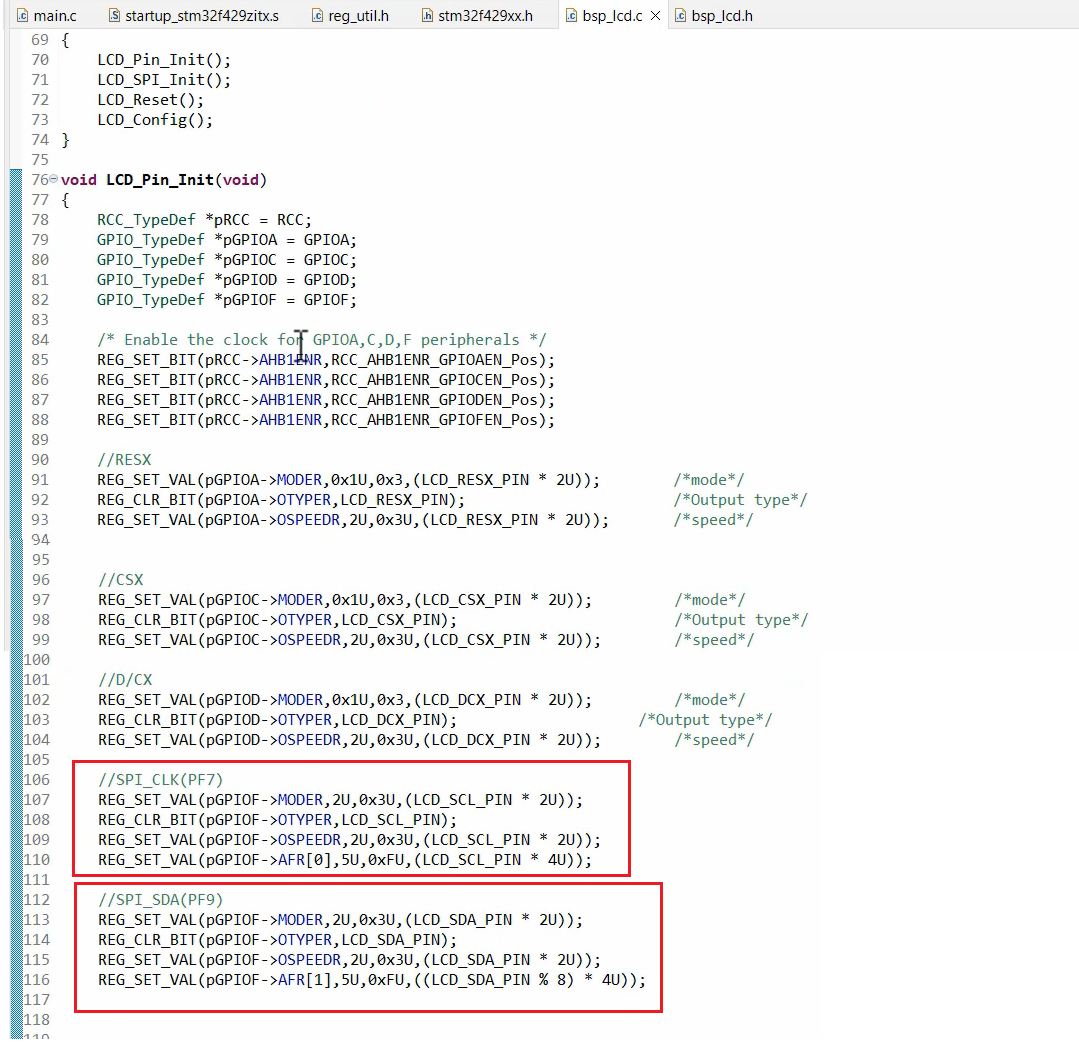
REG_SET_VAL(pGPIOF->MODER,2U, 0x3U, (LCD_SCL_PIN * 2U));
This line sets the mode of a pin, which is connected to the clock signal of an SPI (Serial Peripheral Interface) device, as an output pin with an alternate function mode. The macro REG_SET_VAL is likely a macro that sets the value of a specific bit range in a memory-mapped register. The pGPIOF->MODER pointer likely points to the register that controls the mode of all the pins on a specific GPIO port (port F in this case). 2U specifies the position of the two bits that control the mode of the specific pin being configured, which is calculated by multiplying the pin number (LCD_SCL_PIN) by 2. 0x3U is the value that will be written to those two bits to set the mode to alternate function mode.
REG_CLR_BIT(pGPIOF->OTYPER, LCD_SCL_PIN);
After that, the output type we can keep push-pull. This line clears a bit in the register that controls the output type of a pin, which is connected to the clock signal of the SPI device. The macro REG_CLR_BIT likely takes a pointer to the register and the bit position to be cleared (LCD_SCL_PIN in this case).
REG_SET_VAL(pGPIOF->OSPEEDR, 2U, 0x3U, (LCD_SDA_PIN * 2U));
After that, speed. This line sets the output speed of a pin, which is connected to the data signal of the SPI device, to high speed. The macro REG_SET_VAL likely sets the value of a specific bit range in a memory-mapped register. pGPIOF->OSPEEDR likely points to the register that controls the output speed of all the pins on the GPIO port. 2U specifies the position of the two bits that control the output speed of the specific pin being configured, which is calculated by multiplying the pin number (LCD_SDA_PIN) by 2. 0x3U is the value that will be written to those two bits to set the output speed to high.
REG_SET_VAL(pGPIOF->AFR[1], 5U, 0xFU, ((LCD_SDA_PIN % 8) * 4U));
This line sets the alternate function of a pin, which is connected to the data signal of the SPI device, to a specific function. The macro REG_SET_VAL is likely being used to set the value of a specific bit range in a memory-mapped register. pGPIOF->AFR[1] likely points to the second register in a pair of registers that control the alternate function of all the pins on the GPIO port. 5U specifies the position of the four bits that control the alternate function of the specific pin being configured. 0xFU is the value that will be written to those four bits to select the specific alternate function. ((LCD_SDA_PIN % 8) * 4U) calculates the offset within the register where the four bits for the specific pin being configured are located since each pin’s alternate function is specified by four bits within the register. The %8 operation is used to ensure that the offset is within the range of 0 to 31 since there are 32 bits in each register.
Our LCD_Pin configuration is over.
SPI terminologies
In this article, I will redefine the SPI signal names.
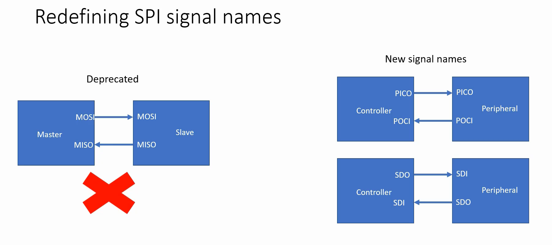
We will not be using master and slave terminology anymore in this article. Instead, we will shift to new signal names. The name “Master” will be replaced with “Controller,” and “Slave” will be replaced with “Peripheral.” Additionally, instead of “MOSI” and “MISO” terminology, you can use “PICO” or “POCI” terminology, or in simpler terms, I will be using the terminology “SDI” and “SDO.” “SDI” stands for “serial data in,” and “SDO” stands for “serial data out.” Please note this change.
MCU SPI peripheral configuration
- Let’s use the below settings for SPI configuration
- SPI mode: Half-duplex Controller
- Data format: 8 bits, msb first
- CPOL and CPHA: Check the peripheral datasheet to obtain the correct setting it requires
- SPI Clock: Check the peripheral datasheet and obtain the max speed it can support(<6Mhz)
- Chip select is handled by the software
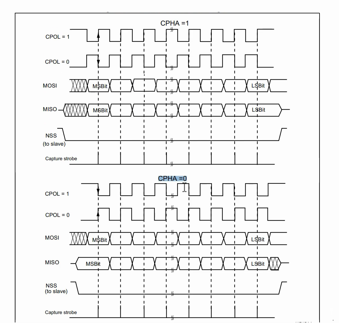
CPOL and CPHA: Check the peripheral datasheet(page number 36) to obtain the correct setting it requires.
CPOL:
CPOL refers to clock polarity, which determines the state of the clock during the IDLE state. When CPOL is set to 0, the IDLE state of the clock will be low. If CPOL is set to 1, the IDLE state will be high. However, if the datasheet specifies CPOL = 0, do not use the alternate polarity.
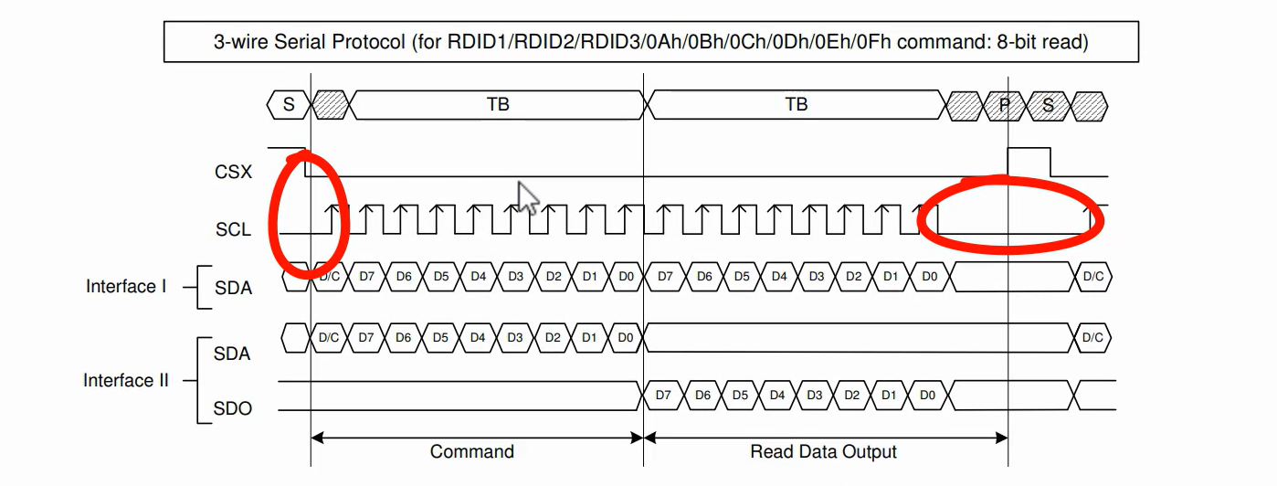
CPHA, or clock phase, determines when data is sampled on the data line. In the timing diagram, the arrow indicates that data is sampled at the rising edge of the clock. This means that the master must update the data in the previous edge of the clock, which occurs when CPHA = 0.
To determine the appropriate settings, refer to the SPI section of the microcontroller’s reference manual, as shown in Figure 10. When CPHA = 0 and CPOL = 0, the controller updates the data on the falling edge and the peripheral samples the data on the rising edge. Therefore, select CPHA as 0 to ensure that the data is correctly updated and sampled. Thus, the recommended settings are CPOL = 0 and CPHA = 0.
SPI Clock
This will be produced by the controller. And you have to check the peripheral datasheet and obtain the maximum speed it can support. You keep the SPI clock speed is less than 6MHz.
Chip select
Chip selection is handled by the software. And there is a dedicated pin for Chip Select, and you have to toggle the chip select whenever you want to activate the peripheral. This is a simple GPIO which we have to toggle.
FastBit Embedded Brain Academy Courses
Click here: https://fastbitlab.com/course1