SPI peripheral configuration coding
In this article, let’s do the SPI_Init function.
Here we do a microcontroller SPI configuration for controller mode.

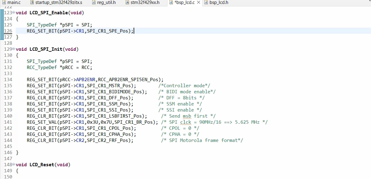
The code provided shows the initialization and configuration of the SPI (Serial Peripheral Interface) peripheral on a microcontroller, as shown in Figure 1.
To begin, we need to activate the peripheral clock for the SPI. The first step is to call the function LCD_SPI_Enable(), which sets the SPE (SPI Enable) bit in the CR1 (Control Register 1) of the SPI peripheral. This function doesn’t require any arguments, but it uses a pointer to the SPI peripheral, which we declare as pSPI. Here’s how the function looks:
void LCD_SPI_Enable(void) {
SPI_TypeDef *pSPI = SPI;
REG_SET_BIT(pSPI->CR1, SPI_CR1_SPE_Pos);
}
This function is called to enable the SPI peripheral for communication with an LCD controller.
The second function, LCD_SPI_Init(), initializes and configures the SPI peripheral.
SPI_TypeDef *pSPI = SPI;
RCC_TypeDef *pRCC = RCC;
These two lines define pointers to the SPI and RCC (Reset and Clock Control) peripheral registers.
The following code lines configure the SPI peripheral. Firstly, the SPI clock is enabled by setting the SPI5EN bit in the AHB2ENR (Advanced High-Performance Bus 2 Enable Register) of the RCC (Reset and Clock Control) peripheral. To do this, it is necessary to locate the SPI5 peripheral on the memory map and determine which bus domain it belongs to. To find this information, refer to the reference manual and navigate to the memory map. It can be observed that in our microcontroller, the SPI5 peripheral is part of the APB2 bus domain.

REG_SET_BIT(pRCC-> AHB2ENR, RCC_APB2ENR_SPI5EN_Pos);
This line sets a bit in the AHB2ENR register of the RCC peripheral to enable the clock for the SPI5 peripheral (this register is used to enable the clock to different peripherals).
Let’s check the SPI registers in the reference manual.

Let’s start with the first register, which is the control register(CR1). Control registers are used to control the peripheral. So, it has various bits here. So, let’s go as per our discussion.
First, set the SPI mode to half-duplex controller mode. Remember, the ‘controller’ is the new word used for ‘master’.
Master selection or controller selection(MSTR):
You have to set this bit. By using this bit, you are telling the SPI that you want to use the SPI as controller mode.

REG_SET_BIT(pSPI->CR1, SPI_CR1_MSTR_Pos);
This line sets the Master Mode bit in the CR1 register of the SPI peripheral. This sets the SPI to operate as the controller (master) in a multi-slave communication system. This is controller mode. But, we need a half-duplex. That you can do using the BIDIMODE.
REG_SET_BIT(pSPI->CR1, SPI_CR1_BIDIMODE_Pos);
This line sets the Bidirectional Data mode bit in the CR1 register of the SPI peripheral. This enables the use of a single wire for both data input and output.
Data frame format (DFF):
We want to use an 8-bit frame format for transmission or reception. Let’s clear this bit.

REG_CLR_BIT(pSPI->CR1, SPI_CR1_DFF_Pos);
This line clears the Data Frame Format bit in the CR1 register of the SPI peripheral. This sets the data frame size to 8 bits.
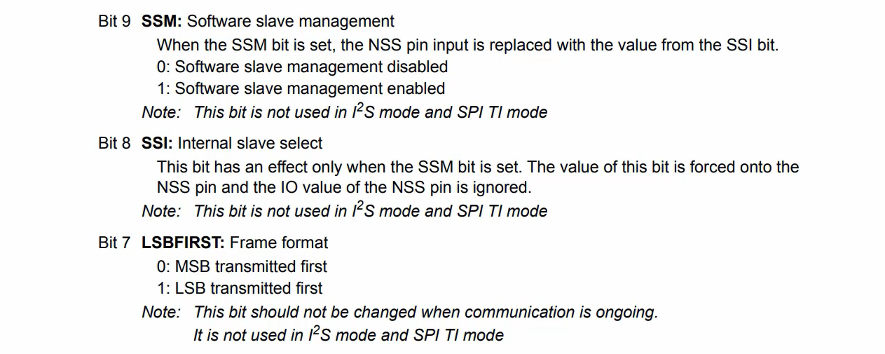
SSM: software slave management
SSM bit has to be enabled. Why? Because, we have our dedicated CS line, which we will be toggling using software. So, we don’t want hardware to manage the peripherals. That’s why you must enable this.

REG_SET_BIT(pSPI->CR1, SPI_CR1_SSM_Pos);
This line sets the Software Slave Management bit in the CR1 register of the SPI peripheral. This allows the master to control the slave selection manually (without using a hardware chip select line).
Internal slave select(SSI):
SSI bit has an effect only when SSM bit is set. So, the value of this bit is forced onto the NSS pin and the value of the NSS pin is ignored.
Don’t worry about this bits, just set this bit to high.
REG_SET_BIT(pSPI->CR1, SPI_CR1_SSI_Pos);
This line sets the Internal Slave Select bit in the CR1 register of the SPI peripheral. This sets the slave select line to a high level, so that the slave device is initially not selected.
LSBFIRST
And after that, we want to send MSB first. So, clear this bit. It just means that, in 8-bit data, so the MSB of the 8-bit that is most significant bit of the frame will be sent on the wire first.
REG_CLR_BIT(pSPI->CR1, SPI_CR1_LSBFIRST_Pos);
This line clears the LSB (Least Significant Bit) first bit in the CR1 register of the SPI peripheral. This sets the transmission order of bits to be sent starting with the MSB (Most Significant Bit).
BR: Baud rate control
Setting the baudrate of the SPI clock is the important part. So, this is generated by the controller.

What is a peripheral clock?
You know that, the SPI5 peripheral lies in the APB2 domain. So, we configured the APB2 bus clock as 90MHz.

To achieve the maximum frequency of 45 MHz, the clock should be divided by 2 since 90 MHz divided by 2 is 45 MHz. However, according to our LCD datasheet, the speed should be less than 6 MHz. To meet this requirement, we need to further divide the clock by 16, which will give us a speed of around 5 MHz.
What happens is, when you select the 011 option(Figure 7), the 90MHz will be divided by 16.
REG_SET_BIT(pSPI->CR1, 0X3U, 0X7U, SPI_CR1_BR_Pos);
This line sets the SPI clock speed in the CR1 register of the SPI peripheral. It uses a bit mask to set the Baud Rate Prescaler (BR) bits to 0x03, which divides the system clock by 16. This sets the SPI clock speed to 90MHz/16 = 5.625MHz, which gives you around 5.625 MHz.
CPOL and CPHA
Now, go to the CPOL and CPHA selection.

Clock Polarity must be 0.
REG_CLR_BIT(pSPI->CR1, SPI_CR1_CPOL_Pos);
This line clears the Clock Polarity bit in the CR1 register of the SPI peripheral. This sets the clock to idle at a low level.
And CPHA must be 0. The first clock transition is the first data capture edge. Let’s use CPHA as 0. This is also called SPI Mode 0.
REG_CLR_BIT(pSPI->CR1, SPI_CR1_CPHA_Pos);
This line clears the Clock Phase bit in the CR1 register of the SPI peripheral. This sets the data to be sampled on the first edge of the clock.
Let’s see whether we have any configuration items in the CR2 register.
You have to select the frame format as SPI Motorola mode. Let’s do that.

REG_CLR_BIT(pSPI->CR2, SPI_CR2_FRF_Pos);
This line clears the Frame Format bit in the CR2 register of the SPI peripheral. This sets the SPI to use the Motorola frame format, which is a standard format used by many devices.
FastBit Embedded Brain Academy Courses
Click here: https://fastbitlab.com/course1


