Testing TFT-LCD command sending
In this article, we initialize the SPI peripheral first and then call the function LCD_SPI_Enable() to activate it.

The code is shown in Figure 1. It just sets the SPE bit of the control register 1. After that, you reset the board and you send commands to the LCD and these are the commands.
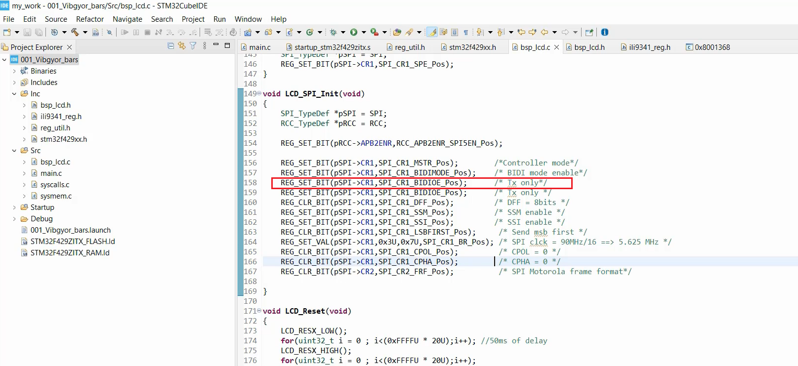
In the LCD_SPI_Init function, we are currently in the controller mode and BIDI mode. However, we have not yet configured whether we want to transmit or receive on the bidirectional data line, which needs to be done separately.
To achieve this, we can use the BIDIOE bit, which is the output enable in bidirectional mode. This bit must be set to 1 whenever we want to transmit data. As we intend to transmit data, we should set this bit to 1.
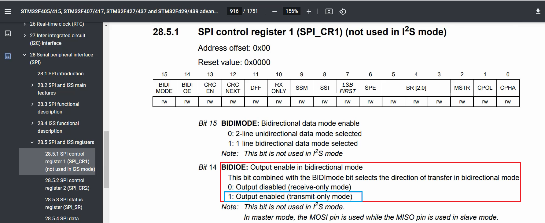
Please make the changes shown in Figure 3 by utilizing the ‘REG_SET_BIT(pSPI->CR1, SPI_CR1_BIDIOE_Pos)‘ function.
You need to connect the logic analyzers to all of the pins to trace the signals. Once this is done, load the code onto the board and activate the IDE’s debug mode. I’ll open the logic analyzer software now.
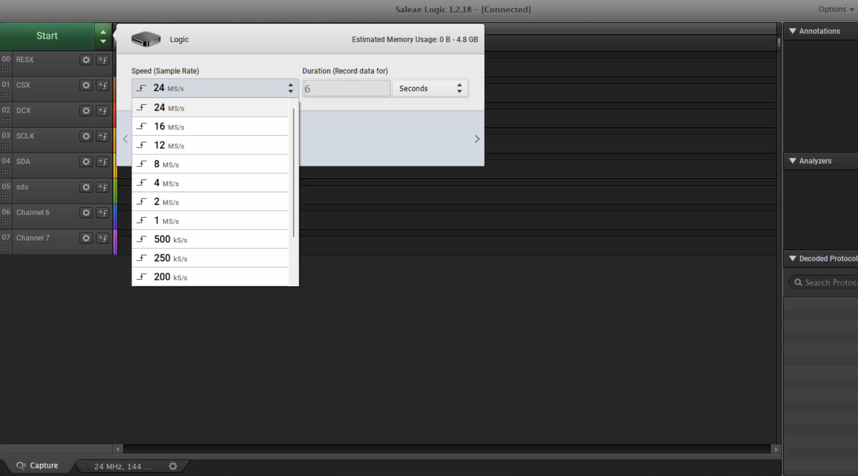
Here I set the sample rate to 24. I’ll select 24, and then let’s click start.
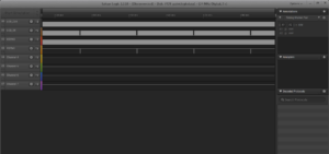
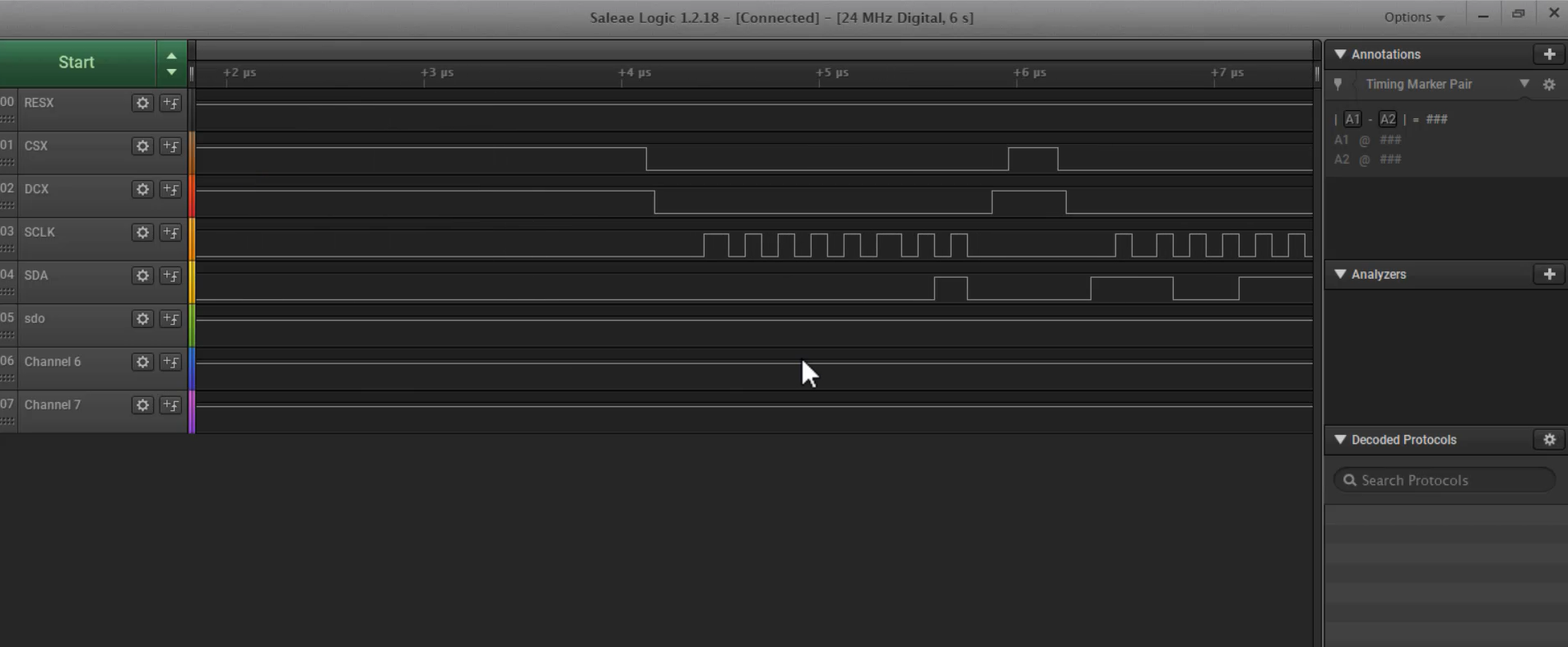
Look at the trace in Figure 5.
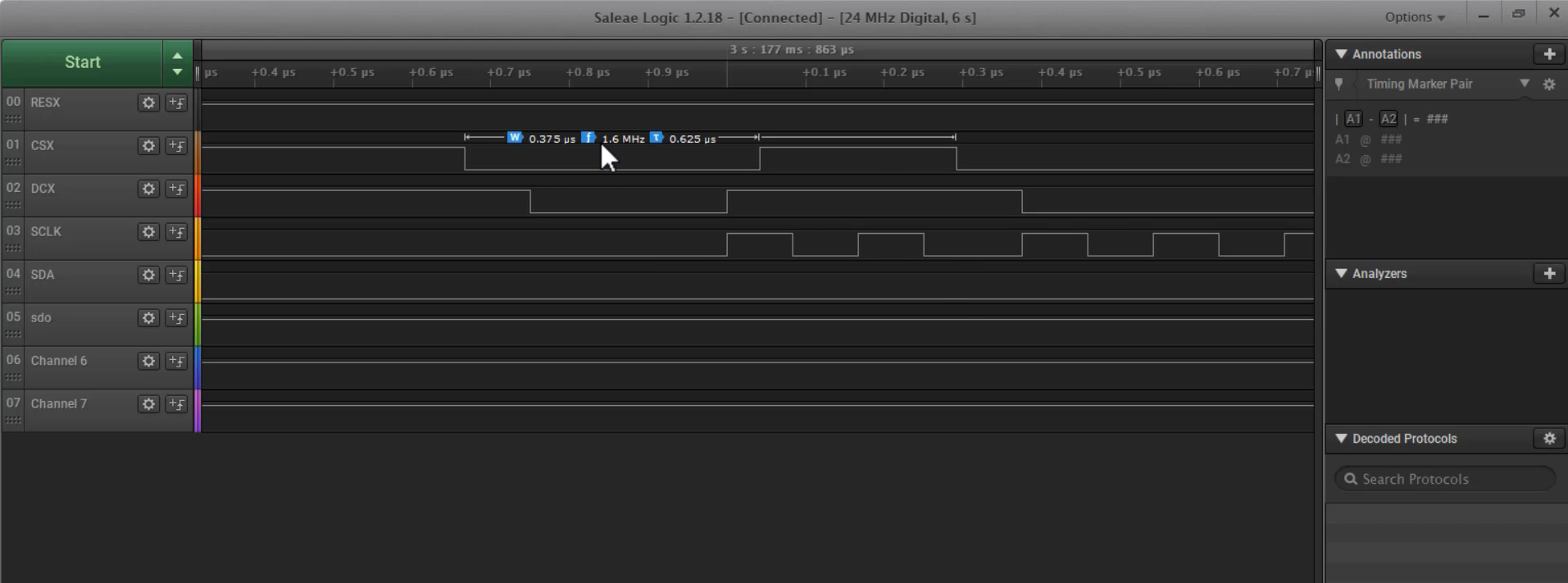
As you can see(Figure 5), this trace appears incorrect. Although we are correctly setting DCX low after making CS low, the clock signal is being generated outside the expected timing. Ideally, data transactions should occur only after the CS line has been asserted to low, but it appears to be happening outside of that boundary in this case. This indicates that there may be an issue with our code.
There is actually a mistake that I made here, which is mentioned in the reference manual. You can check the SR for the Busy flag.
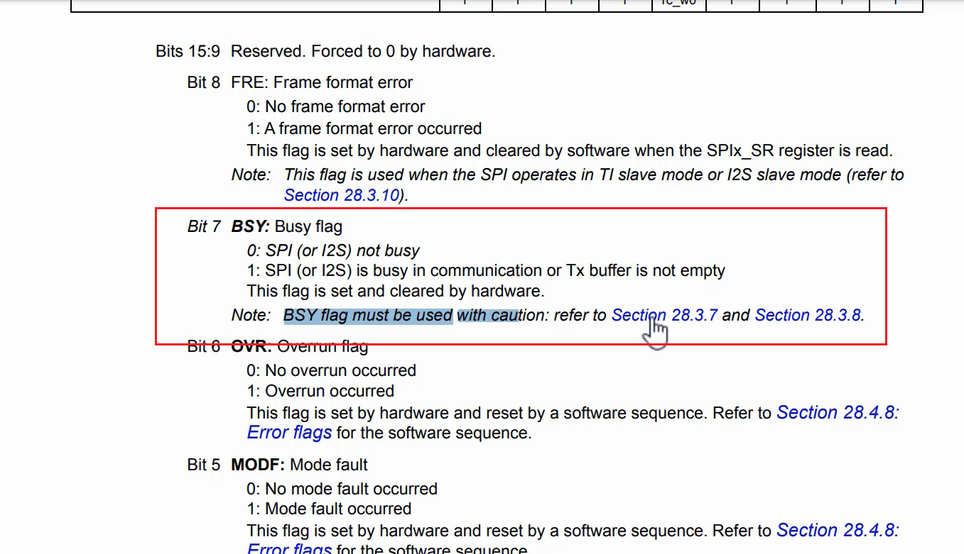
Busy flag must be used with caution: refer to section 28.3.7 for more information.
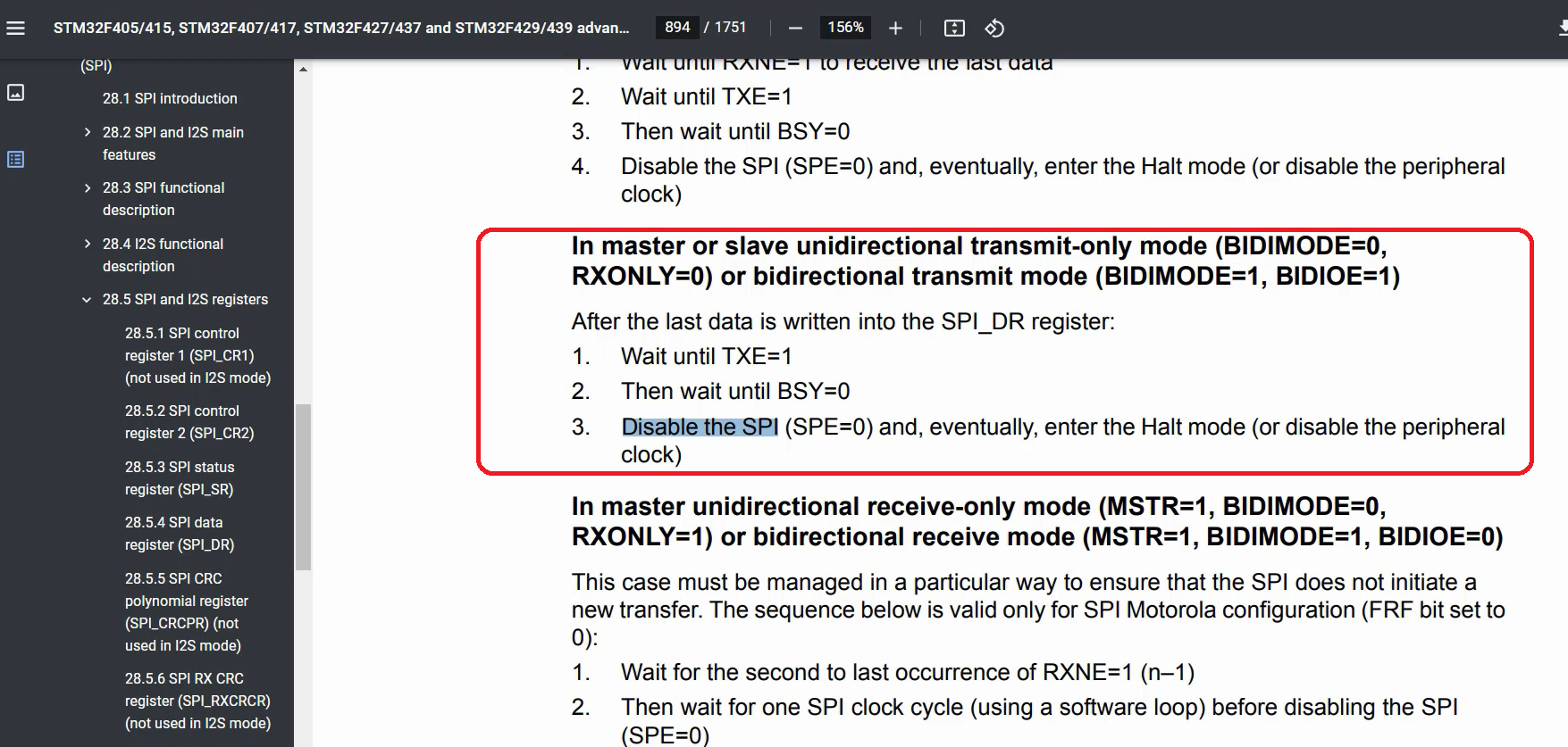
Here you can see that, when BIDIMODE = 1, and BIDIOE=1, wait until TXE =1, so this we are not doing.
After the last data is written into the SPI_DR register:
- wait until TXE = 1,
- then wait until BSY = 0,
- Disable the SPI (SPE=0) and, eventually, enter the Halt mode. (You can conclude that it is the end of the transfer)
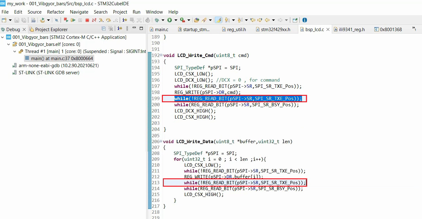
Let’s go back to our bsp_lcd.c code, and here we will add the following line.
while(!REG_READ_BIT(pSPI->SR, SPI_SR_TXE_Pos)); (line 199 and 213, as shown in Figure 8).
Let’s take a look at the trace. I’ll reset the board first.
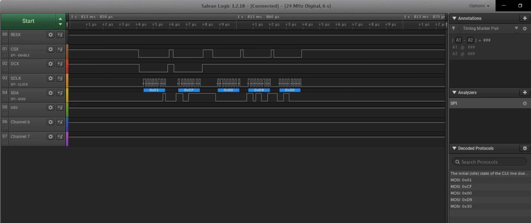
Look at Figure 9, now it is happening correctly. So, the transaction is happening inside this CS assertion.
To decode the data line, navigate to the Analyzers section and select SPI. MOSI is referred to as SDA, so select number 4 – ‘SDA’. However, MISO is not present, so select ‘None’. Clock is number 3 – ‘SCLK’, and Enable is number 1 – ‘CSX’. MSB is transmitted first, 8 bits per transfer, CPOL = 0, CPHA is 0. Finally, click on ‘Save’.

Look at Figure 11, it decoded the data line.
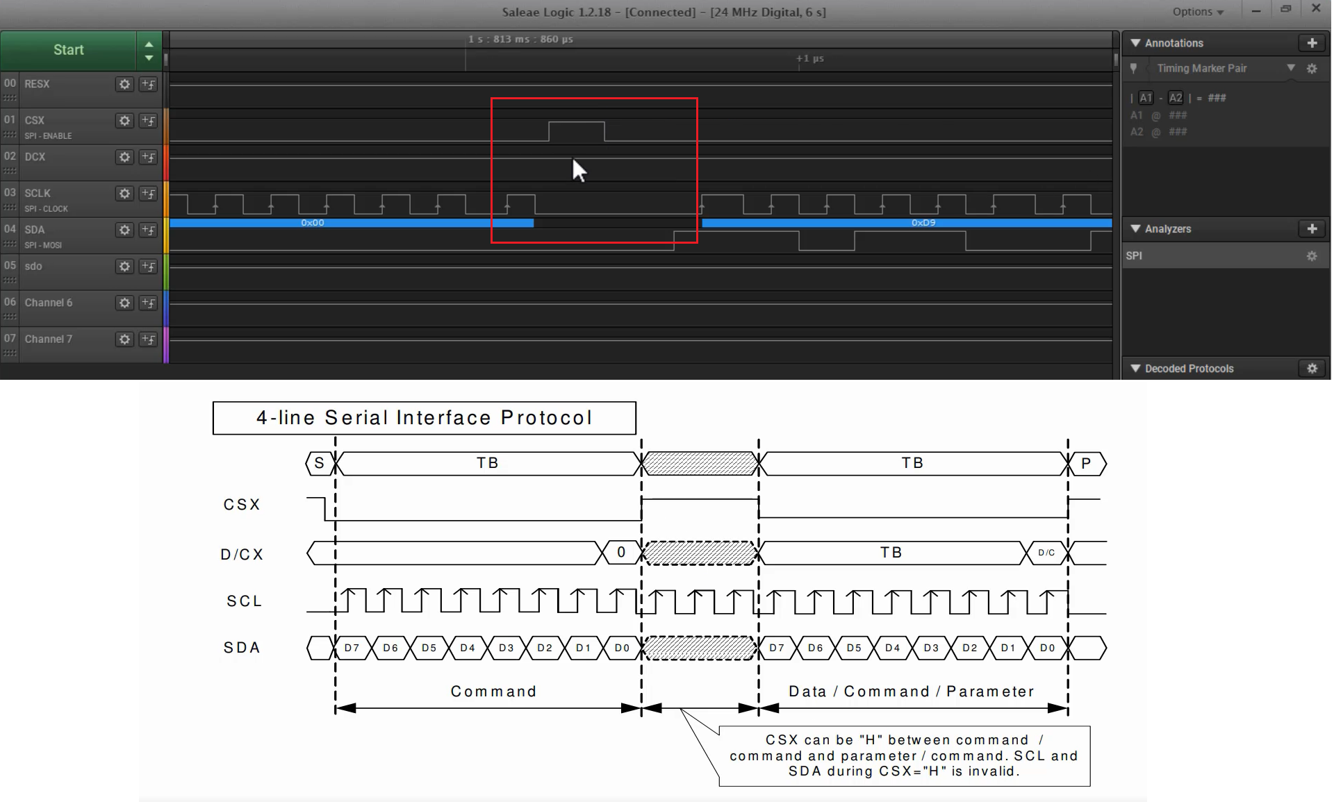
Is it necessary to raise the CS signal between parameter transfers?
I think you can keep this low. You need not deassert and assert again. Because, if you check the timing diagram in the datasheet of ILI9341, and page number 35. It says CSX can be “High” between command/command and parameter/command. SCL and SDA during CSX-’H’ is invalid.
FastBit Embedded Brain Academy Courses
Click here: https://fastbitlab.com/course1

