SPI behind the scene data communication principle
In this article, let’s understand how data communication takes place between master and slave devices.
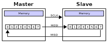
From Figure 1. SPI peripheral of the microcontroller consists of a shift register. So, SPI communication based on the shift registers.
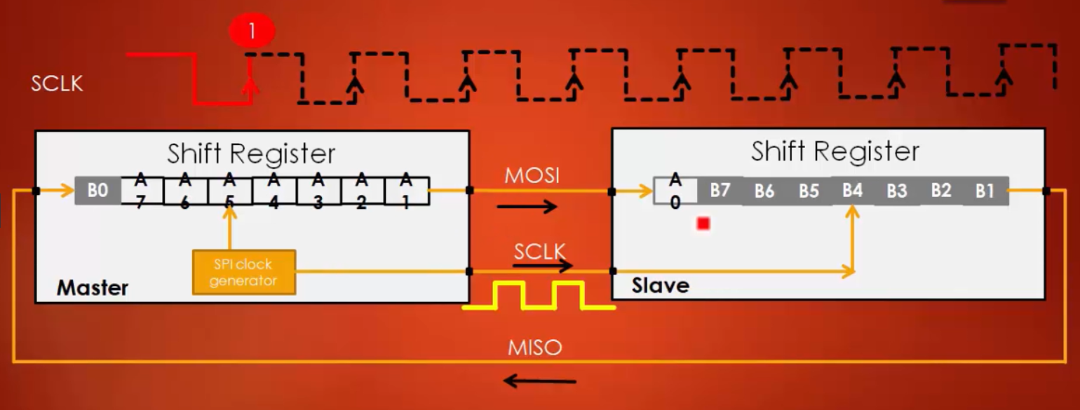
From Figure 2. There are two devices one is the master, and another one is the slave.
The master SPI peripheral has one shift-register of 8-bits, and the slave SPI peripheral has one shift-register of 8-bits. Transmissions typically involve two shift registers of some given word-size, such as eight bits, one in the master and one in the slave.
However, other word-sizes are also common, for example, 16-bit words for touch-screen controllers or audio codecs, such as the TSC2101 by Texas Instruments, or 12-bit words for many digital-to-analog or analog-to-digital converters.
MOSI of the master connected to the MOSI of the slave. The clock pins are related, and the MISO of the master connected to the MISO of the slave. SPI is a synchronous serial communication protocol. So, the clock is required to send the data or push the data.
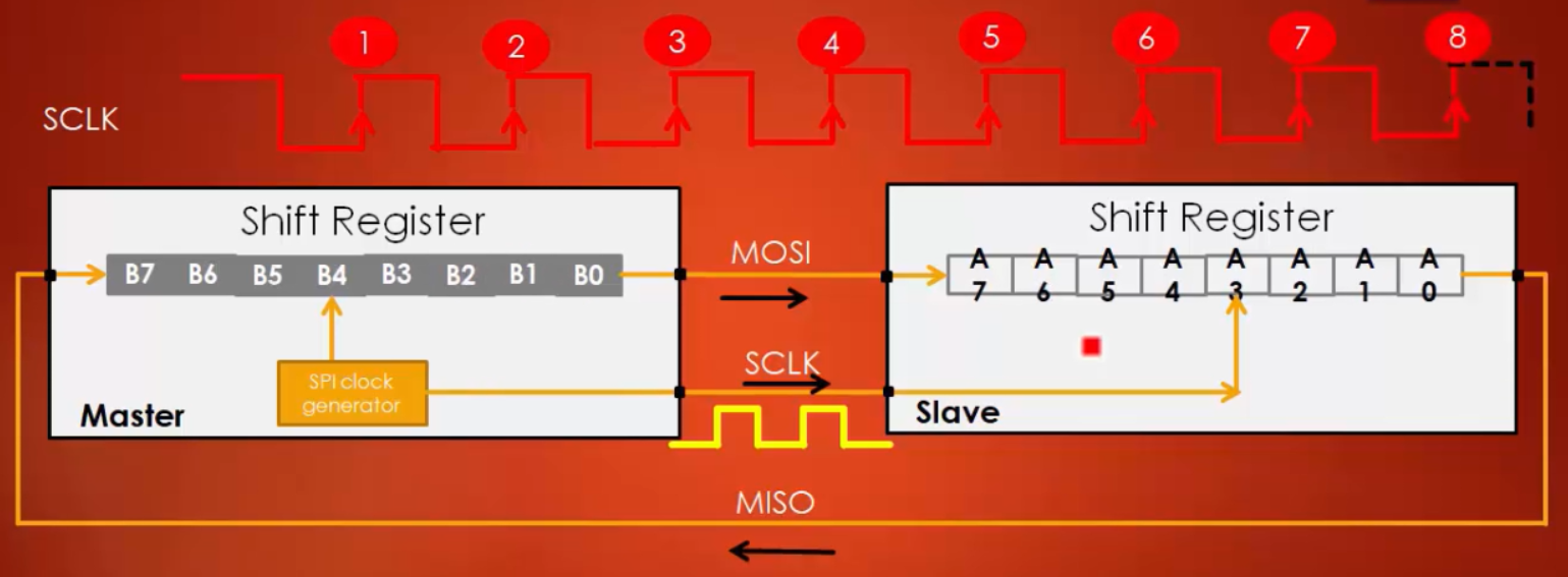
Let’s send the data which is there in the master shift-register to the slave shift-register. Initially, data A0-A7 are there in the shift register of the master device, and B0-B7 is there in the shift register of the slave device. After one clock cycle A0 which is there on LSB is moved out of the MOSI line and it reached the MSB position of the slave shift register.
So, the data transferred by one clock cycle. The last data B0 of the slave shift register moved out of the MISO line, and it settled in the MSB position of the master shift register. So, for every clock cycle, there will be a shift in the shift register.
In the following article, let’s learn SPI Bus configuration: Full duplex, Half-duplex, and Simplex.
FastBit Embedded Brain Academy Courses
Click here: https://fastbitlab.com/course1

