SPI functional block diagram explanation
The SPI allows synchronous, serial communication between the MCU and external devices.
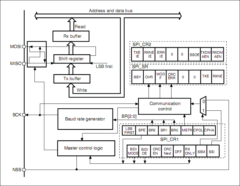
SPI functional block diagram of the STM32F407x microcontroller:
Most of ST’s microcontroller have similar SPI block diagram. The main elements of SPI and their interactions are shown in the following block diagram Figure 1.

From Figure 1, SPI peripheral has four pins they are NSS pin, SCK pin, MISO, and MOSI pin. These four I/O pins are dedicated to SPI communication with external devices.
In the block diagram of SPI, there is a shift register. In ST’s case shift register width is upto 16 bits. Hence SPI peripheral supports data communication of 16 bits. Here shift registers are connected to the MOSI and MISO lines.
If the SPI peripheral working as master and then data will be shifted out from shift register and it will go to the external world over the MOSI line. If the SPI peripheral is receiving the data from the outer world over the MISO line and it will get into the shift register. The baud rate generator controlled the Clock pin if the peripheral is master. Baud rate generator can configure using baud rate settings (BR[2:0]). Baud rate settings are in baud rate setting bits, which are there in the control register (SPI_CR1).
There are two buffers, one is a Tx buffer, and the other one is Rx buffer.
These buffers can access from the APB bus ( Address and a data bus). Whenever a shift register receives some data, then that data will be moved to Rx buffer. Then read the data from Rx buffer. To transmit some data, then that data write into the Tx buffer. The firmware writes the data into a Tx buffer.
If the shift register is free, that means SPI is not busy in communication, whatever data loaded into the Tx buffer will be moved to shift register. And the transmission begins. From the shift register, data will run out of the MOSI pin.
FastBit Embedded Brain Academy Courses,
Click here: https://fastbitlab.com/course1


