I2C Functional block diagram

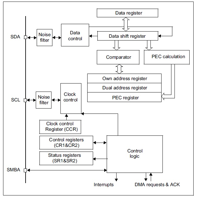
In this article, let’s discuss the block diagram of I2C. The block diagram of I2C is same in all the ST’s microcontroller.
In the block diagram, there are mainly three pins:
- SDA
- SCL
- SMBA.
SMBA is an optional signal in SMBus mode, and this signal is not applicable if SMBus is disabled. SMBus provides a control bus for system and power management related tasks. Both SDA and SCL pins are preceded by a noise filter which is used to remove some glitches or spikes etc. The noise filter is used to smoothen the SDA and SCL signals.
I2C is a half-duplex communication because there is only one data register in the block diagram of I2C.
The data register is connected to the data shift register. So, the firmware or code is going to write data into the data register, and then data register contents are copied to the data shift register.
From the data shift register, the data will be transmitted to the external world. When data comes from the outer world, the data goes to the data shift register, and when one complete byte is received, the data will be copied to the data register. The data read from the data register.
I2C peripheral can be used either in master mode or in slave mode. When I2C peripheral is configured in slave mode, then slave address stored in the own address register as shown in Figure 1. The own address register is applicable only when the device is in slave mode, and this register is used to store the slave address. The SCL pin is connected to the clock control block, and the clock control block is connected to the clock control register(CCR). By configuring clock control, register one can produce different frequencies on the serial clock (SCL) pin.
In the following article, let’s see I2C driver API requirements.
FastBit Embedded Brain Academy Courses,
Click here: https://fastbitlab.com/course1


