I2C ACK and NACK and I2C data validity
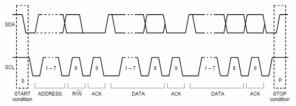
In this article, let’s discuss the I2C ACK, NACK, and I2C data validity.
Data on the I2C bus is transferred in 8-bit packets (bytes). There is no limitation on the number of bytes.
However, each byte must be followed by an Acknowledge bit. This bit signals whether the device is ready to proceed with the next byte. For all data bits, including the Acknowledge bit, the master must generate clock pulses. If the slave device does not acknowledge the transfer, this means that there is no more data or the device is not ready for the assignment yet. The master device must either generate a STOP or Repeated START condition.
From Figure 1. Consider the address phase of the I2C bus protocol. The first 7-bits are slave addresses, and the 8th one is a read-write bit. In the 8th clock cycle of SCL, the SDA is 1, which means read operation. Suppose if the SDA is 0, then write operation.
Let’s understand about ACKing and NACKing. The 9th clock cycle of SCL is for the ACKing and NACKing. The acknowledge signal is defined as the transmitter releases the SDA line during the acknowledge clock pulse. So, the receiver can pull the SDA line low, and it remains stable low during the high period of the clock pulse. If the SDA line is drawn to high, then that is NACK. So, when the SDA line is high during the 9th clock pulse of the SCL, this is called not acknowledge signal.
After NACK, the master can generate either the STOP condition to abort the transfer or a repeated START condition to start a new transmission.
In simple words, ACKing and NACKing are defined as, during the 9th clock pulse of SCL, if the SDA line is low, then it is accepted as ACK, and if the SDA line is high then it is acceptable as NACK. So, the acknowledge takes place after every byte. The acknowledge bit allows the receiver to signal the transmitter that the byte was successfully received and ready to receive another byte. The master generates all clock pulse, including acknowledging in the 9th clock pulse. So, the transmitter always expects the ACK or NACK during the 9th clock cycle.
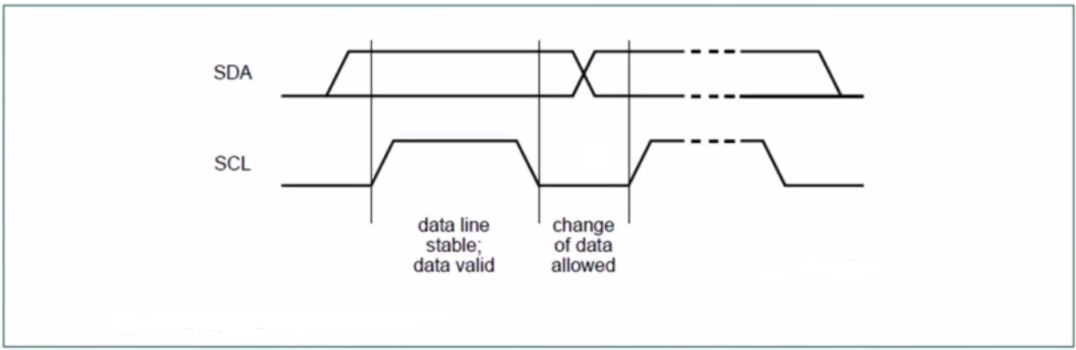
From Figure 2. Each master must generate its clock signal, and the data can change only when the clock is low. The high or low state of the data can change when the clock signal on the SCL is low. So, the change means either from 0 to 1 or 1 to 0.
In I2C, data should not change when the clock is high. But this does not apply to the START and STOP condition. So, any transitions happen when the clock is high is detected as either the START and STOP condition. Thus, the data is valid only when the clock is high.